- Mark as New
- Bookmark
- Subscribe
- Mute
- Subscribe to RSS Feed
- Permalink
- Report Inappropriate Content
Device - Stratix IV
Using PCIe x4 Gen2. For the purpose of Transceiver offset cancelation I am using the external alt_gx_reconfig. I have been using a PLL output to feed this clock and using the pll_locked as the reset generator. Like this, altgx_reconfig altgx_0_reconfig ( .offset_cancellation_reset(~pll_locked), // pll locked .reconfig_clk (pll_clk_50), // clock from PLL .reconfig_fromgxb (reconfig_0_fromgxb), .busy (busy), .reconfig_togxb (reconfig_togxb) ); This works perfectly. But I need to free up this PLL and use for another purpose and I am thinking of using a clock coming directly from the pin. And I am not quite sure what to do with the reset, I tried to ground the reset altogether which made the PCIe not to come up at all. Now I am thinking the pcie reset could be connected to the altgx_reconfig. Like this, altgx_reconfig altgx_0_reconfig ( .offset_cancellation_reset (~pcie_rstn), // PCIe reset .reconfig_clk (clkin_50), // clock coming from a x'tal .reconfig_fromgxb (reconfig_0_fromgxb), .busy (busy), .reconfig_togxb (reconfig_togxb) ); But that did not work either. PCI express is not responding. Any ideas what I could do?Link Copied
- Mark as New
- Bookmark
- Subscribe
- Mute
- Subscribe to RSS Feed
- Permalink
- Report Inappropriate Content
--- Quote Start --- For the purpose of Transceiver offset cancelation I am using the external alt_gx_reconfig. I have been using a PLL output to feed this clock and using the pll_locked as the reset generator. Like this, altgx_reconfig altgx_0_reconfig ( .offset_cancellation_reset(~pll_locked), // pll locked .reconfig_clk (pll_clk_50), // clock from PLL .reconfig_fromgxb (reconfig_0_fromgxb), .busy (busy), .reconfig_togxb (reconfig_togxb) ); This works perfectly. --- Quote End --- But it is wrong. You should not control the reset signal with a signal that is not deglitched, eg., see Altera's KB example http://www.altera.com/support/kdb/solutions/rd12172009_309.html and the SignalTap II traces in the PDF associated with this thread: http://www.alteraforum.com/forum/showthread.php?t=35678 --- Quote Start --- But I need to free up this PLL and use for another purpose and I am thinking of using a clock coming directly from the pin. And I am not quite sure what to do with the reset --- Quote End --- You could tie it to an on-board power-on reset source. --- Quote Start --- Now I am thinking the pcie reset could be connected to the altgx_reconfig. Like this, altgx_reconfig altgx_0_reconfig ( .offset_cancellation_reset (~pcie_rstn), // PCIe reset .reconfig_clk (clkin_50), // clock coming from a x'tal .reconfig_fromgxb (reconfig_0_fromgxb), .busy (busy), .reconfig_togxb (reconfig_togxb) ); But that did not work either. PCI express is not responding. --- Quote End --- That is because the PCIe core needs to start link training as soon as reset deasserts, eg., see p5 of this doc for the requirements. http://www.ovro.caltech.edu/~dwh/wbsddc/ts4_power.pdf You need to tie the reset to something that deasserts once the FPGA is configured, eg., a reset supervisor input, or an internally generated signal that asserts and then deasserts at power-on. Cheers, Dave
- Mark as New
- Bookmark
- Subscribe
- Mute
- Subscribe to RSS Feed
- Permalink
- Report Inappropriate Content
Thanks Dave! I had in fact gone through the document you mentioned about deglitching the reset, but I didn't experience any issues so far without it, I guess I was just lucky.
I will try to use an internally generated reset pulse and see if that works. I will post the results tomorrow. And I have to read this, good document http://www.ovro.caltech.edu/~dwh/wbsddc/ts4_power.pdf. Thanks!- Mark as New
- Bookmark
- Subscribe
- Mute
- Subscribe to RSS Feed
- Permalink
- Report Inappropriate Content
Hmm.. Something is still wrong. I did create a power on reset type signal internally. I can see in signal tap that the reset to altgx_reconfig block is assserted (see picture) and kept for about 640ns, alt_gx_reconfig_busy is asserted and I also see that it is deasserted later on(not in the picture), dont know after how long(I am going to try to signaltap and see when the pci reset is asserted and when the busy is deasserted).
https://www.alteraforum.com/forum/attachment.php?attachmentid=7016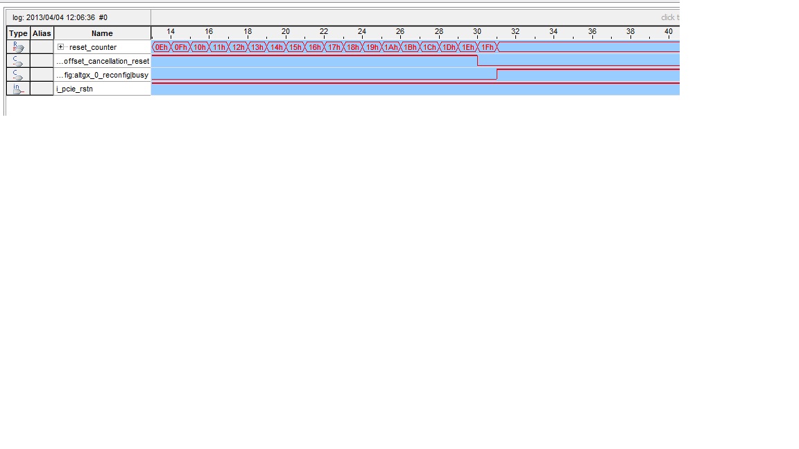
- Mark as New
- Bookmark
- Subscribe
- Mute
- Subscribe to RSS Feed
- Permalink
- Report Inappropriate Content
--- Quote Start --- Hmm.. Something is still wrong. I did create a power on reset type signal internally. I can see in signal tap that the reset to altgx_reconfig block is assserted (see picture) and kept for about 640ns, alt_gx_reconfig_busy is asserted and I also see that it is deasserted later on(not in the picture), dont know after how long(I am going to try to signaltap and see when the pci reset is asserted and when the busy is deasserted). --- Quote End --- The Qsys PCIe thread that I linked to above has some SignalTap II traces. I recently posted some ALTGX/ALTGX_CONFIG traces in this thread too: http://www.alteraforum.com/forum/showthread.php?t=40144 http://www.alteraforum.com/forum/attachment.php?attachmentid=6985&d=1364498035 Cheers, Dave
- Mark as New
- Bookmark
- Subscribe
- Mute
- Subscribe to RSS Feed
- Permalink
- Report Inappropriate Content
Ok, I think I got it to work. The issue was that the time the reset was asserted was too short. I increased it from 640ns to about 8.5us and looks like the PCIe interface is working. I will keep an eye on it and needs more verification, but looks like that was it. Thanks Dave for the documents and information.
https://www.alteraforum.com/forum/attachment.php?attachmentid=7030
- Mark as New
- Bookmark
- Subscribe
- Mute
- Subscribe to RSS Feed
- Permalink
- Report Inappropriate Content
Your SignalTap II trace still does not look correct. Your trace shows pcie_rstn high, i.e., deasserted. Offset cancellation should have completed long before reset deasserts, i.e., I would expect to see pcie_rstn low in your traces.
Cheers, Dave- Mark as New
- Bookmark
- Subscribe
- Mute
- Subscribe to RSS Feed
- Permalink
- Report Inappropriate Content
--- Quote Start --- Your SignalTap II trace still does not look correct. Your trace shows pcie_rstn high, i.e., deasserted. Offset cancellation should have completed long before reset deasserts, i.e., I would expect to see pcie_rstn low in your traces. Cheers, Dave --- Quote End --- Let me see if I understand this correctly. I think the sequence of events is, 1. Powerup of FPGA (PCIe reset is not yet asserted) 2. FPGA Config done 3. altgx_reconfig block gets the reset and goes busy (as in my signaltap) and starts the transciever calibration. 4. altgx_reconfig busy gets deasserted. ready for PCIe handshke with root complex. 5. All these steps up until now shouldnt take more than 100ms. Now the PCIe_rst_n is asserted. And the PCIe hard IP resets and ready for transfer 6. PCIe enumeration... blah blah blah 7. PCIe pkt transfers goes on. So pcie reset gets asserted after the 100ms time after powerup, my signaltap show the activity just after the fpga config done where pcie reset should be deasserted and will be asserted later on. Am I Correct? Or were you asking why I dont have the pcie_rstn low in my signaltap towards the end of it? I only have only captured 8k samples after powerup(160us)
- Mark as New
- Bookmark
- Subscribe
- Mute
- Subscribe to RSS Feed
- Permalink
- Report Inappropriate Content
--- Quote Start --- Let me see if I understand this correctly. I think the sequence of events is, 1. Powerup of FPGA (PCIe reset is not yet asserted) 2. FPGA Config done 3. altgx_reconfig block gets the reset and goes busy (as in my signaltap) and starts the transciever calibration. 4. altgx_reconfig busy gets deasserted. ready for PCIe handshke with root complex. --- Quote End --- The ts4_power.pdf I linked to has the power-on sequence. PCIe is supposed to be asserted by the host. It should asserted for steps 1-4 --- Quote Start --- 5. All these steps up until now shouldnt take more than 100ms. Now the PCIe_rst_n is asserted. And the PCIe hard IP resets and ready for transfer --- Quote End --- They won't take less than 100ms, but they could take longer - again, look at the diagram I have already referred you to. --- Quote Start --- So pcie reset gets asserted after the 100ms time after powerup --- Quote End --- PCIe reset should be asserted any time you trigger from power-up - see the diagram on p5 of the doc. --- Quote Start --- my signaltap show the activity just after the fpga config done where pcie reset should be deasserted and will be asserted later on. Am I Correct? --- Quote End --- Its possible that your host does not assert reset at power on, even though it should. This would be analogous to what would happen if you just hit the reset button on your host CPU. But even in that case, the host should assert the reset in the sequence shown in the diagram I linked to. The document lists all the references to the specifications that have those timing requirements listed. --- Quote Start --- Or were you asking why I dont have the pcie_rstn low in my signaltap towards the end of it? I only have only captured 8k samples after powerup(160us) --- Quote End --- Grab an oscilloscope and look at the timing of your reset. Its not necessarily wrong, its just something that is worth looking at and paying attention to. This will save you from debugging a problem with your hardware, when infact its your host that is in violation of the specifications. Note: If you do always see PCIe reset deasserted in your traces, then check the timing of your FPGA configuration controller. If the configuration controller for this board was designed incorrectly, the FPGA may be taking too long to configure. For example, the FPGA should be configured via Fast Passive Parallel or Passive Serial (with a faster clock than Active Serial), and almost never via Active Serial (since it takes too long) Cheers, Dave
- Mark as New
- Bookmark
- Subscribe
- Mute
- Subscribe to RSS Feed
- Permalink
- Report Inappropriate Content
Thanks again Dave!
Let me get back and do some more checking, I was thinking that the reset might be pulled up high at power-on and host asserts the reset once the BIOS chip is powered up and host starts its enumeration sequence. I will check more on the timing aspect of things and get back with more data, And thanks for sharing the documents, its a really good one. I need to read that.- Mark as New
- Bookmark
- Subscribe
- Mute
- Subscribe to RSS Feed
- Permalink
- Report Inappropriate Content
--- Quote Start --- Let me get back and do some more checking, I was thinking that the reset might be pulled up high at power-on and host asserts the reset once the BIOS chip is powered up and host starts its enumeration sequence. I will check more on the timing aspect of things and get back with more data, --- Quote End --- Its quite possible that is the case, and it would probably be acceptable. Its worth poking around in your hardware to get a sense of what is going on at the system level, and then write your testbenches to match that and several other power-up sequences to see if your design behaves correctly. Cheers, Dave
- Mark as New
- Bookmark
- Subscribe
- Mute
- Subscribe to RSS Feed
- Permalink
- Report Inappropriate Content
--- Quote Start --- Its quite possible that is the case, and it would probably be acceptable. Its worth poking around in your hardware to get a sense of what is going on at the system level, and then write your testbenches to match that and several other power-up sequences to see if your design behaves correctly. Cheers, Dave --- Quote End --- Ok so, I got some more data. Seems like after cold boot of the host PC, PCIe reset is asserted for almost ~500ms (see the pic, signal captured). C1(yellow) is the pcie reset and c2 (pink) is the Vcc. https://www.alteraforum.com/forum/attachment.php?attachmentid=7064 But when I restart the PC, the reset is asserted only for a ~5ms, I am not sure if there is another reset coming after this, but I doubt it. See the pic below https://www.alteraforum.com/forum/attachment.php?attachmentid=7065 So I think my signaltap in the earlier post shows that the pci reset occured long before the FPGA configuration finished and thats the reason I am not seeing reset being asserted in the waveform. That also means that I am not really getting a proper reset to my FPGA logic (except for the PCIe hard IP block) since all my logic resets are connected to the pcie reset (except for the altgx_reconfig block for which I generated a reset internally).
- Mark as New
- Bookmark
- Subscribe
- Mute
- Subscribe to RSS Feed
- Permalink
- Report Inappropriate Content
--- Quote Start --- Ok so, I got some more data. --- Quote End --- Great! Thanks. These are reasonable waveforms. Keep in mind that the FPGA offset cancellation routine only ever runs when the FPGA is first configured, eg., when its powered or reprogrammed via JTAG or another configuration source. After that point, the ALTGX_RECONFIG busy signal will not assert right after reconfig_reset or offset_cancellation_reset deasserts to indicate offset cancellation is running. Note: that if you reconfigured your FPGA using JTAG, pressed the reset button, and then took the SignalTap II traces, you would see the ALTGX_RECONFIG busy signal asserted while offset cancellation is running, and PCIe reset would be deasserted (if you missed the 5ms low time of the signal). --- Quote Start --- So I think my signaltap in the earlier post shows that the pci reset occured long before the FPGA configuration finished and thats the reason I am not seeing reset being asserted in the waveform. --- Quote End --- Its possible. But if those plots were also showing offset cancellation running (busy high), the reset signal should be low (if it was a power-on SignalTap II trace). --- Quote Start --- That also means that I am not really getting a proper reset to my FPGA logic (except for the PCIe hard IP block) since all my logic resets are connected to the pcie reset (except for the altgx_reconfig block for which I generated a reset internally). --- Quote End --- 5ms is more than long enough for a reset. The PCIe reset should be passed through reset synchronizers that asynchronously assert and synchronously deassert for each of the clock domains in your design that PCIe reset is supposed to reset. Assuming all of these clocks are in the MHz range, 5ms is thousands of clocks. Is the PCIe interface working in either or both of these reset sequences/conditions? If the power-on-reset is not working, then probe CONF_DONE to see when your FPGA is configured relative to PCIe reset deasserting. Cheers, Dave
- Mark as New
- Bookmark
- Subscribe
- Mute
- Subscribe to RSS Feed
- Permalink
- Report Inappropriate Content
--- Quote Start --- Great! Thanks. These are reasonable waveforms. Keep in mind that the FPGA offset cancellation routine only ever runs when the FPGA is first configured, eg., when its powered or reprogrammed via JTAG or another configuration source. After that point, the ALTGX_RECONFIG busy signal will not assert right after reconfig_reset or offset_cancellation_reset deasserts to indicate offset cancellation is running. Note: that if you reconfigured your FPGA using JTAG, pressed the reset button, and then took the SignalTap II traces, you would see the ALTGX_RECONFIG busy signal asserted while offset cancellation is running, and PCIe reset would be deasserted (if you missed the 5ms low time of the signal). --- Quote End --- Its not loaded through JTAG, but is configured by the CPLD on powerup, I flashed the binary. In my case, I dont have any other reset other than PCIe reset (No reset button/other POR). So on PERST# assertion, CPLD programs the FPGA and since the reprogramming will take more than 5ms (FPP), by the time config is done, the PERST# reset would already have been deasserted in the case of a PC Reset. --- Quote Start --- Its possible. But if those plots were also showing offset cancellation running (busy high), the reset signal should be low (if it was a power-on SignalTap II trace). --- Quote End --- Yes, it was a Power-on signaltap. Offset cancellation went busy after my internally generated reset was asserted, but I never saw the PCIe reset being asserted in my signaltap. --- Quote Start --- 5ms is more than long enough for a reset. The PCIe reset should be passed through reset synchronizers that asynchronously assert and synchronously deassert for each of the clock domains in your design that PCIe reset is supposed to reset. Assuming all of these clocks are in the MHz range, 5ms is thousands of clocks. --- Quote End --- Yes, but since I am programming the FPGA on this reset, once config is done, reset would have already deaaserted. --- Quote Start --- Is the PCIe interface working in either or both of these reset sequences/conditions? --- Quote End --- Yes, PCIe interface seems to be working fine. Enumeration is done and device is transferring data. The only thing I am unable to do is to cause a re-enumeration without restarting the PC. (For eg. if I reprogram the FPGA via JTAG, and try to access the PCIe interface, it would not be recognized, since the enumeration is happening only during powerup/reboot). Any idea, if there is a way I can achieve that? Hotplug?/warm reset? --- Quote Start --- If the power-on-reset is not working, then probe CONF_DONE to see when your FPGA is configured relative to PCIe reset deasserting. --- Quote End --- I was trying to do that, but unfortunately I dont have any vias on the board to probe on conf_done. All I could get my probe on was the nConfig signal (config start), which as you would expect is happening at the reset edge.
- Mark as New
- Bookmark
- Subscribe
- Mute
- Subscribe to RSS Feed
- Permalink
- Report Inappropriate Content
--- Quote Start --- on PERST# assertion, CPLD programs the FPGA --- Quote End --- This is not the correct solution. When the CPLD first powers on, it should program the FPGA. There is no need to program the FPGA when PERST# asserts. --- Quote Start --- The only thing I am unable to do is to cause a re-enumeration without restarting the PC. (For eg. if I reprogram the FPGA via JTAG, and try to access the PCIe interface, it would not be recognized, since the enumeration is happening only during powerup/reboot). Any idea, if there is a way I can achieve that? Hotplug?/warm reset? --- Quote End --- Yeah, you can use hot-plug under Linux. I'm not sure about Windows. --- Quote Start --- I was trying to do that, but unfortunately I dont have any vias on the board to probe on conf_done. All I could get my probe on was the nConfig signal (config start), which as you would expect is happening at the reset edge. --- Quote End --- If you are using a CPLD to program the FPGA, then you should have a pretty good idea as to how long programming will take. So how long is that? Cheers, Dave
- Mark as New
- Bookmark
- Subscribe
- Mute
- Subscribe to RSS Feed
- Permalink
- Report Inappropriate Content
--- Quote Start --- When the CPLD first powers on, it should program the FPGA. There is no need to program the FPGA when PERST# asserts. --- Quote End --- You are right, I had it that way before, but faced some issues with binary update at site when the host PC just does a warm boot after a system update. So now I just put it to update every time there is a PCIe reset. --- Quote Start --- Yeah, you can use hot-plug under Linux. I'm not sure about Windows. --- Quote End --- I would like to understand how to do that(in linux), Can you please point me to any docs? or give some more info, Thanks! We have PC platform, but I may get some idea. --- Quote Start --- If you are using a CPLD to program the FPGA, then you should have a pretty good idea as to how long programming will take. So how long is that? --- Quote End --- I had to check it.. Its taking about 600ms, and since there is an internal delay or something on a powerup, it takes more than a sec (1100ms) after powerup before the FPGA is programmed and ready. So definitely I am missing the pcie reset (in both cases, PC Cold Boot/Warm boot) I attached the waveforms as well. So, I am going to generate a reset after the PCIe reset and the reconfiguration. PC after Cold Boot (there is a mistake in signal name, pink is fpga config done) https://www.alteraforum.com/forum/attachment.php?attachmentid=7070 PC After Warm boot https://www.alteraforum.com/forum/attachment.php?attachmentid=7071 PC After Warm Boot - Zoomed to show the PERST# since its only a 5ms. https://www.alteraforum.com/forum/attachment.php?attachmentid=7072
- Mark as New
- Bookmark
- Subscribe
- Mute
- Subscribe to RSS Feed
- Permalink
- Report Inappropriate Content
--- Quote Start --- You are right, I had it that way before, but faced some issues with binary update at site when the host PC just does a warm boot after a system update. So now I just put it to update every time there is a PCIe reset. --- Quote End --- This "fix" is causing you other problems, so really you need to fix this problem first. --- Quote Start --- I would like to understand how to do that(in linux), Can you please point me to any docs? or give some more info, Thanks! We have PC platform, but I may get some idea. --- Quote End --- Send me an email to my forum name and I'll forward an email discussion that I had on this topic. --- Quote Start --- I had to check it.. Its taking about 600ms, and since there is an internal delay or something on a powerup, it takes more than a sec (1100ms) after powerup before the FPGA is programmed and ready. --- Quote End --- This is not good. You need to determine all of your power on timing delay sources, eg., look at your on-board power-supplies, their ramp times, etc. Your board may be violating the power-on-requirements of the FPGA, i.e., hiding even more issues. --- Quote Start --- So definitely I am missing the pcie reset (in both cases, PC Cold Boot/Warm boot) I attached the waveforms as well. So, I am going to generate a reset after the PCIe reset and the reconfiguration. --- Quote End --- Generating another reset is not going to help. What you are not looking at in these traces is the PCIe bus activity. Your PCIe end-point will miss the traffic on the bus that configures it. If its working in this motherboard, then its just luck. The next motherboard you plug it into, it may not work. The "solution" is to; 1) Configure the FPGA at power-on "as fast as possible", ideally within 100ms, but if you cannot achieve that, then faster than the deassertion of PCIe reset. 2) Do not reconfigure when PCIe reset asserts. There is no reason to. The FPGA just needs to treat the PCIe reset as a reset source. You don't have to reset all logic within the FPGA if you do not want to, eg., you can have a "last reset reason" register that sets a power-on bit at power on, and a PCIe reset bit when PCIe reset occurs (of course if your FPGA configures faster than PCIe reset deasserts, then you'll only ever see the PCIe reset bit set). Cheers, Dave
- Mark as New
- Bookmark
- Subscribe
- Mute
- Subscribe to RSS Feed
- Permalink
- Report Inappropriate Content
--- Quote Start --- This "fix" is causing you other problems, so really you need to fix this problem first. Send me an email to my forum name and I'll forward an email discussion that I had on this topic. This is not good. You need to determine all of your power on timing delay sources, eg., look at your on-board power-supplies, their ramp times, etc. Your board may be violating the power-on-requirements of the FPGA, i.e., hiding even more issues. --- Quote End --- Thanks. I am going to look at why there is that significant delay during cold boot than on a warm boot. --- Quote Start --- Generating another reset is not going to help. What you are not looking at in these traces is the PCIe bus activity. Your PCIe end-point will miss the traffic on the bus that configures it. If its working in this motherboard, then its just luck. The next motherboard you plug it into, it may not work. The "solution" is to; 1) Configure the FPGA at power-on "as fast as possible", ideally within 100ms, but if you cannot achieve that, then faster than the deassertion of PCIe reset. --- Quote End --- I checked the CPLD, we are using a 50MHz clock and Flash access time(from where the data is fetched by CPLD) is about 70ns, and due to that each byte is taking about 100ns to be sent to the FPGA during configuration. The configuration data for our device is about 6MBytes and that explains why CPLD takes about 600ms to finish the reconfiguration. Yes, I still need to check why there is some extra time taken on a cold boot, but I may not still be able reconfigure the FPGA within 100ms, or not even 500ms. --- Quote Start --- 2) Do not reconfigure when PCIe reset asserts. There is no reason to. --- Quote End --- Yeah, I agree. I am going to make the change, Thanks! --- Quote Start --- The FPGA just needs to treat the PCIe reset as a reset source. You don't have to reset all logic within the FPGA if you do not want to, eg., you can have a "last reset reason" register that sets a power-on bit at power on, and a PCIe reset bit when PCIe reset occurs (of course if your FPGA configures faster than PCIe reset deasserts, then you'll only ever see the PCIe reset bit set). Cheers, Dave --- Quote End ---
- Mark as New
- Bookmark
- Subscribe
- Mute
- Subscribe to RSS Feed
- Permalink
- Report Inappropriate Content
--- Quote Start --- I checked the CPLD, we are using a 50MHz clock and Flash access time (from where the data is fetched by CPLD) is about 70ns, and due to that each byte is taking about 100ns to be sent to the FPGA during configuration. The configuration data for our device is about 6MBytes and that explains why CPLD takes about 600ms to finish the reconfiguration. Yes, I still need to check why there is some extra time taken on a cold boot, but I may not still be able reconfigure the FPGA within 100ms, or not even 500ms. --- Quote End --- Ok, so this is a design "feature" then. This complicates the use of this board, since it will work in some motherboards, but not others. The board designer's responsibility is to perform a timing analysis (like the one in the doc I linked to) and as shown in this doc: http://www.ovro.caltech.edu/~dwh/carma_board/fpga_configuration.pdf For example, see the timing diagram on p30 where 16-bit flash reads are used to program an FPGA in FPP mode. The flash read access timing is what limits the design. Using page-mode flash helps. Review your design. Perhaps the board has page mode flash, and you're not using that feature. That might allow you to speed things up slightly. Cheers, Dave
- Mark as New
- Bookmark
- Subscribe
- Mute
- Subscribe to RSS Feed
- Permalink
- Report Inappropriate Content
I sent an email to you.
--- Quote Start --- Ok, so this is a design "feature" then. This complicates the use of this board, since it will work in some motherboards, but not others. --- Quote End --- This board is not sold separately, but is part of a larger system, so it is integrated with a known (tested) motherboard in all situations. And since we are using hard IP, (which would be up and running at powerup), even though configuration is delayed, the PC is able to talk to the hard IP and get it enumerated once PCIe reset is deasserted (even though I am wondering how it is working with a late algx_reconfig_reset). EDIT : I think my statement not be true. Even though its a hardIP implemetation, FPGA reconfiguration has to be finished for the PCIe hardIP to respond to config read requests from the motherboard? --- Quote Start --- The board designer's responsibility is to perform a timing analysis (like the one in the doc I linked to) and as shown in this doc: http://www.ovro.caltech.edu/~dwh/carma_board/fpga_configuration.pdf For example, see the timing diagram on p30 where 16-bit flash reads are used to program an FPGA in FPP mode. The flash read access timing is what limits the design. Using page-mode flash helps. Review your design. Perhaps the board has page mode flash, and you're not using that feature. That might allow you to speed things up slightly. Cheers, Dave --- Quote End --- Yes, I have M29EW flash device (micron), and it supports the page buffer read mode (with 25ns read access time), but seems like the PFL doesnt have that option. I only have a spansion page mode access (in advanced read mode) listed, which gave me a slight improvement in read latency, but it still takes more than 500ms to configure the FPGA. I found out why there is an added delay during powerup, it was because the configuration was only starting once the FPGA reset was deasseted (since the PFL was configured to reprogram on pcie reset), Once I removed it, the fpga programming takes about ~600ms, still outside the reset assertion. Thanks for sharing the document.- Mark as New
- Bookmark
- Subscribe
- Mute
- Subscribe to RSS Feed
- Permalink
- Report Inappropriate Content
--- Quote Start --- I sent an email to you. --- Quote End --- I've responded to it. --- Quote Start --- This board is not sold separately, but is part of a larger system, so it is integrated with a known (tested) motherboard in all situations. --- Quote End --- Great. Then your job now is to document these timing requirements, and the requirements for the motherboard. If you do not do this now, some poor soul (perhaps yourself) will have to figure out why things are not working with "the new motherboards" some time in the future. --- Quote Start --- FPGA reconfiguration has to be finished for the PCIe hardIP to respond to config read requests from the motherboard? --- Quote End --- FPGA reconfiguration and link training has to be complete - the details are in the timing figure I referred you to earlier. --- Quote Start --- Yes, I have M29EW flash device (micron), and it supports the page buffer read mode (with 25ns read access time), but seems like the PFL doesnt have that option. I only have a spansion page mode access (in advanced read mode) listed, which gave me a slight improvement in read latency, but it still takes more than 500ms to configure the FPGA. --- Quote End --- Ignore what PFL gives you. Do the math. What is the fastest you should be able to configure the FPGA? If the best you can do is close to this number, then there is no reason to change the implementation. However, even if you find you can make it faster, you do not need to (since your motherboard is ok with the current timing). Just document that the design could be improved, and show how. Later if this product needs to be revised, these types of changes can be made. Cheers, Dave
- Subscribe to RSS Feed
- Mark Topic as New
- Mark Topic as Read
- Float this Topic for Current User
- Bookmark
- Subscribe
- Printer Friendly Page