- Mark as New
- Bookmark
- Subscribe
- Mute
- Subscribe to RSS Feed
- Permalink
- Report Inappropriate Content
We are trying to leverage the arria 10 CvP (Configuration Via Protocol) feature into the current project. So far we have followed the steps as per user guide ug_a10_cvp_prop.pdf
As part of the process, we are splitting the sof into periph.jic (for flash) and core.rbf (for Host). We have been successful programming both the files and configure the FPGA.
However, We are not getting image displayed on SDI output. We narrow down the issue to the block (video_output) which is responsible for displaying the SDI video.
It contains intel IP core and few VHDL/Verilog custom blocks. Below are the list of intel IP core used in the video_output block
- Transceiver Native PHY Intel Arria 10/Cyclone 10 FPGA IP
- fPLL Intel Arria 10/Cyclone 10 FPGA IP
- Transceiver PHY Reset Controller Intel FPGA IP
Note : When CvP is disabled video output block works just fine and we get the video through SDI output
Here are my thoughts :
- I suspect while splitting the sof into periph.jic and core.rbf some portion of the periph image is not correctly being created due to some wrong tool setting (Conflict with CvP settings)
- Intel IP or transceivers may be violating some power on timing condition when CvP is enable with specific FPGA initialization sequence (load Peripheral image from flash first and then host sends the core image).
Could anyone please share your thoughts and help us investigating/supporting this issue ?
I am monitoring the internals of the video_output block (related to intel IP). I will keep you posted with new updates.
- Mark as New
- Bookmark
- Subscribe
- Mute
- Subscribe to RSS Feed
- Permalink
- Report Inappropriate Content
Hi Chee pin and John
I followed the steps mentioned in section 7.5.2. Fractional PLL Recalibration of ug_arria10_xcvr_phy.pdf
I implemented the system console command sequence as below :
# Follow these steps to re calibrate the fPLL:
# Request user access to the internal configuration bus by writing 0x2 to offset address 0x0[7:0]
#::ist::write_tcvr_pll_reg 0x000 2
#Wait for reconfig_waitrequest to be deasserted (logic low) or wait until capability register of PreSICE Avalon memory-mapped interface control0x280[2]=0x0
#::ist::read_tcvr_pll_reg 0x280
#To calibrate the fPLL, Read-Modify-Write 0x1 to bit[1] of address 0x100 of the fPLL
#::ist::write_tcvr_pll_reg 0x100 2
#Release the internal configuration bus to PreSICE to perform recalibration by writing 0x1 to offset address 0x0[7:0]
#::ist::write_tcvr_pll_reg 0x000 1
I do get the fPLL lock and SDI output is up and running successfully.
I really appreciate your suggestions
Regards,
Piyush,
Regards,
Piyush.
Link Copied
- Mark as New
- Bookmark
- Subscribe
- Mute
- Subscribe to RSS Feed
- Permalink
- Report Inappropriate Content
Hi,
May I know if you have try to reset the SDI IP and also monitor the SDI IP signal using SignalTap?
- Mark as New
- Bookmark
- Subscribe
- Mute
- Subscribe to RSS Feed
- Permalink
- Report Inappropriate Content
Yes, I tried resetting the SDI IP but no luck. The ready status from Transceiver PHY reset controller ramains low (which is why I am not getting the SDI video output).
So currently I am monitoring other signals like PLL locked, cal_busy for PLL and transceiver PHY, just to make sure the calibration is done. I also have to make sure that the transceiver went through correct reset sequence.
I will keep you posted with more information soon.
Do I have to do something specific for transceiver calibration and transceiver reset sequence as far as CvP initialization mode is concern ?
- Mark as New
- Bookmark
- Subscribe
- Mute
- Subscribe to RSS Feed
- Permalink
- Report Inappropriate Content
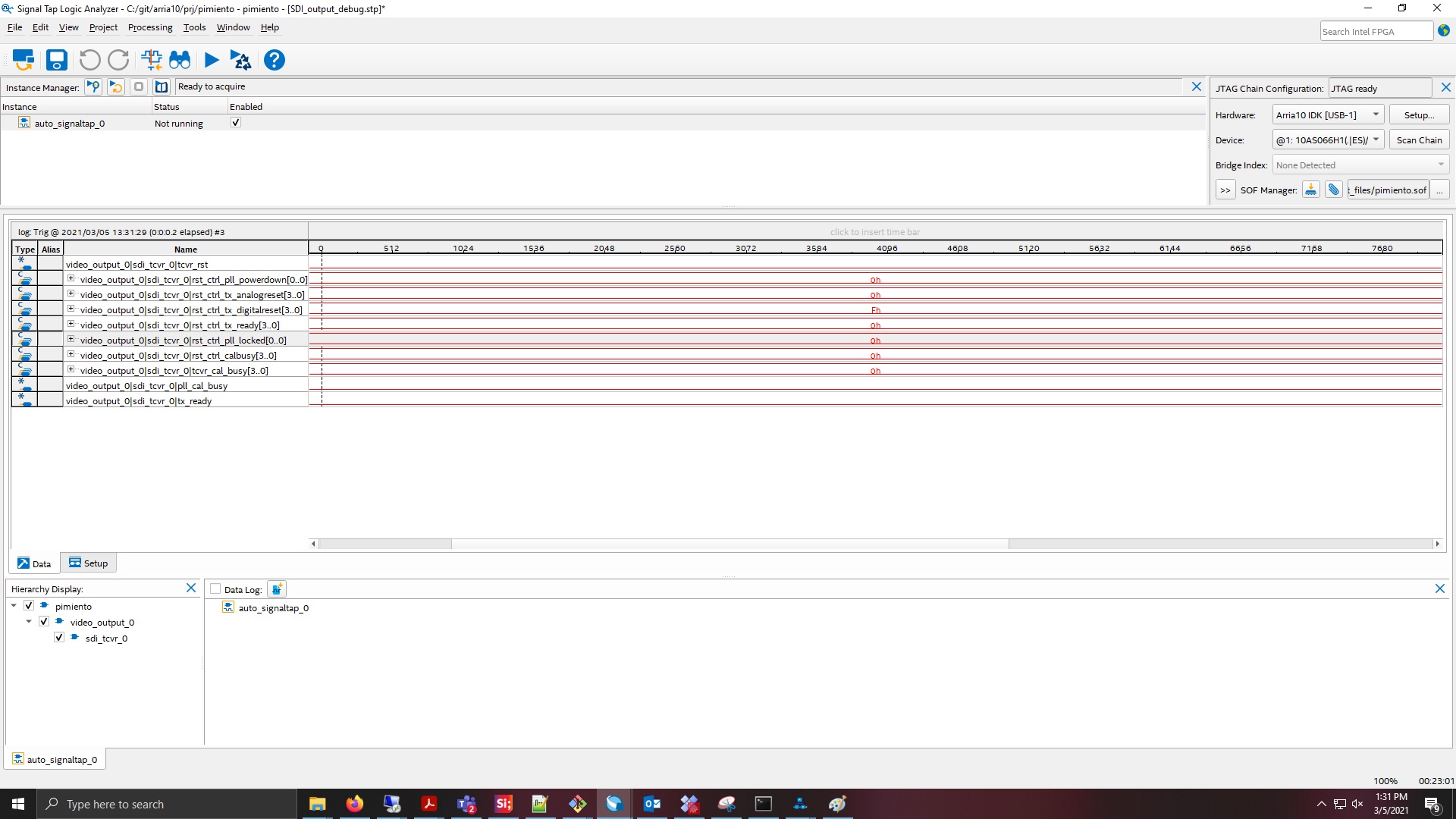
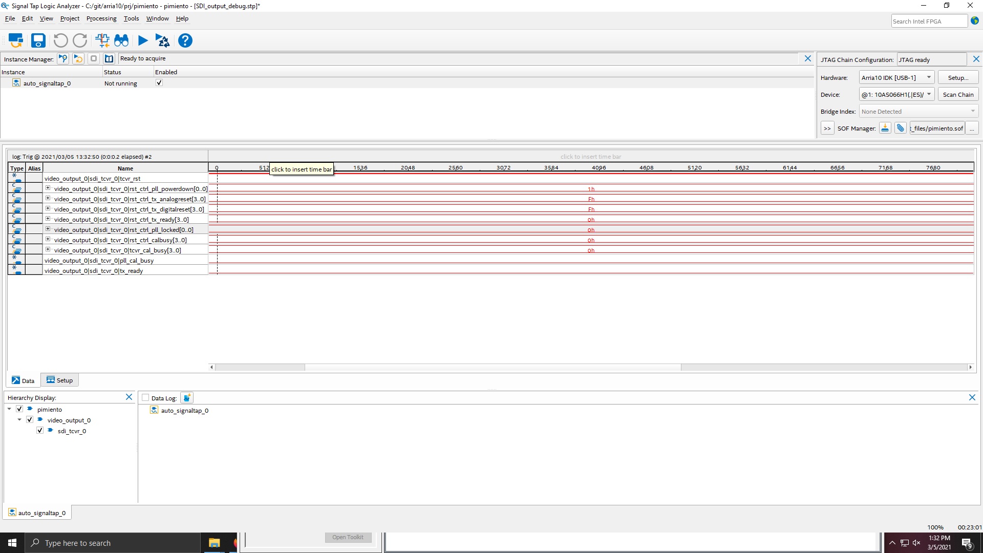
After CvP initialization is Done, capture SDI PLL and reset transceiver signals in Signal Tap
1. When SDI is working (Without CvP enabled - programming normal *.sof) tx_ready is high and PLL is locked - see attached capture "Working Condition PLL Locked.JPG" and other signals are also in correct state.
2.When SDI is not working (CvP Enabled) tx_ready is low and PLL is not locked, digital reset is high from transceiver reset (may be due to missing lock input) - see attached capture "Not Working no PLL lock Digital reset high"
3. I verifed the PLL input clock (148.5 MHz) using oscilloscope, in fact I am using the same clock as sample clock in signal tap. I also try resetting the reset controller which drives the the pll_powerdown input, still not getting the PLL lock after de assertion of reset- see attached "pll_powerdown active.jpg"
It seems PLL lock is the issue, However, In all cases busy signal remains low ? does that mean the calibration is successfully done during CvP initialization?
Any thoughts ?? Thanks.
- Mark as New
- Bookmark
- Subscribe
- Mute
- Subscribe to RSS Feed
- Permalink
- Report Inappropriate Content
Hi,
Just would like to confirm if the design already enter user mode when you are checking the SignalTap? Could you help to check why the digitalreset is high?
Have you try to reset the SDI after you enter user mode to see if it is able to recover?
- Mark as New
- Bookmark
- Subscribe
- Mute
- Subscribe to RSS Feed
- Permalink
- Report Inappropriate Content
Hi JohnT,
Thank you for your response.
Yes, Design is already enter into user mode when I am checking the SignalTap.
I think the reason for digital reset is high from PHY reset controller IP is because the PLL lock (input) signal is low from PLL IP.
I tried resetting the SDI after FPGA enters into user mode, it doesn't recover and digital reset remains high with no PLL lock.
- Mark as New
- Bookmark
- Subscribe
- Mute
- Subscribe to RSS Feed
- Permalink
- Report Inappropriate Content
Hi,
May I know if you are running the same board when testing the design? Could you share with me your Quartus Project for CvP so that I can further look into the issue?
- Mark as New
- Bookmark
- Subscribe
- Mute
- Subscribe to RSS Feed
- Permalink
- Report Inappropriate Content
Yes, I am running the same board when testing the design. After entering into user mode, only SDI output doesn't work when CvP is enabled and rest of the FPGA logic works fine .
When building the same project without CvP enabled works just fine including SDI.
I will share the Quartus project with CvP enabled for your review.
Thanks
- Mark as New
- Bookmark
- Subscribe
- Mute
- Subscribe to RSS Feed
- Permalink
- Report Inappropriate Content
Please find the attached CvP_SDI_Issue.zip for your review.
Project was build in Quartus 19.3. Please advice. Let me know if you need any more info.
- Mark as New
- Bookmark
- Subscribe
- Mute
- Subscribe to RSS Feed
- Permalink
- Report Inappropriate Content
Hi John,
I just wanted to follow up on the SDI project that I shared few days back.
Please review and see if you can provide any suggestions/workaround.
Appreciate you support.
Regards,
Piyush.
- Mark as New
- Bookmark
- Subscribe
- Mute
- Subscribe to RSS Feed
- Permalink
- Report Inappropriate Content
Hi,
Sorry for the delay as I am still in the progress of investigate the issue to figure out what went wrong.
- Mark as New
- Bookmark
- Subscribe
- Mute
- Subscribe to RSS Feed
- Permalink
- Report Inappropriate Content
Hi,
I am Chee Pin and will be working together with John to assist you on this case. I will be focusing on the fPLL not lock perspective.
Please see my responses as following:
1. As I understand it, you mentioned that you have tried to perform a reset to the fPLL using the pll_powerdown input port. Not sure if you are aware of it, by default the A10 fPLL internal reset signal is controlled by AVMM register but not the pll_powerdown input port. You can refer to the following KDB for further details:
Can you try to reset the fPLL by writing to fPLL reset register ie 0x2E0[0] to see if there is any difference? You can monitor the pll_cal_busy and pll_locked after you writing to the reset register.
2. If the above is not working, you can try to perform a fPLL recalibration followed by reset to see if it helps.
3. Regarding your inquiry if the calibration has succeeded, you may check on the following:
i. In signaltap, after programming, you should observed pll_cal_busy high and then go low to indicate calibration has taken place
ii. Please ensure the fPLL refclk and CLKUSR are directly sourced from stable and free-running oscillators on-board. These signals need to be stable and free-running prior to device power up.
Please let me know if there is any concern. Thank you.
- Mark as New
- Bookmark
- Subscribe
- Mute
- Subscribe to RSS Feed
- Permalink
- Report Inappropriate Content
Thank you Chee Pin for your response and provide me detailed steps to debug the fPLL lock
Followed below steps so far :
1. Try web case (workaround/fix): changed the QSF assignment to change the reset control from the Avalon-MM register to the pll_powerdown input: This did not help and still no lock when I toggle the pll_powerdown input
2.Implement Avalon-MM register Interface : Enable the dynamic reconfiguration interface and enable control and status registers and add custom Avalon control interface IP to access the fPLL registers. Update the fPLL block and make appropriate port connection and build the project.
Please review below settings and ports:

3.Try to reset the fPLL by toggling to fPLL reset register i.e. 0x2E0[0] , no change is observed in pll_cal_busy and pll_locked signals

Just to make sure I am correctly accessing the fPLL registers, I read few registers and get some default values, can you confirm if these values are correct
system console commands
% ist::read_tcvr_pll_reg 0x0
0x00000002
% ist::read_tcvr_pll_reg 0x1
0x00000001
% ist::read_tcvr_pll_reg 0x2
0x00000000
% ist::read_tcvr_pll_reg 0x3
0x00000000
when I write '1' into 0x2E0 command and read back I get the correct value
% ist::write_tcvr_pll_reg 0x2E0 1
% ist::read_tcvr_pll_reg 0x2E0
0x00000001
when I write '0' into 0x2E0 command and read back I get the correct value
% ist::write_tcvr_pll_reg 0x2E0 0
% ist::read_tcvr_pll_reg 0x2E0
0x00000000
4. Next step is to try reconfigure the fPLL, Could you refer some documentation or steps for fPLL reconfiguration process ?
fPLL refclk and CLKUSR are directly sourced from stable and free-running oscillators on-board and they seems to be good because everything is working when CvP mode is disabled.
Regards,
Piyush.
- Mark as New
- Bookmark
- Subscribe
- Mute
- Subscribe to RSS Feed
- Permalink
- Report Inappropriate Content
Signal tap Write/Read command Captures
Write command

Read command

No fPLL lock, so I will continue exploring the fPLL reconfiguration as suggested by Chee Pin.
Regards,
Piyush.
- Mark as New
- Bookmark
- Subscribe
- Mute
- Subscribe to RSS Feed
- Permalink
- Report Inappropriate Content
Hi Chee pin and John
I followed the steps mentioned in section 7.5.2. Fractional PLL Recalibration of ug_arria10_xcvr_phy.pdf
I implemented the system console command sequence as below :
# Follow these steps to re calibrate the fPLL:
# Request user access to the internal configuration bus by writing 0x2 to offset address 0x0[7:0]
#::ist::write_tcvr_pll_reg 0x000 2
#Wait for reconfig_waitrequest to be deasserted (logic low) or wait until capability register of PreSICE Avalon memory-mapped interface control0x280[2]=0x0
#::ist::read_tcvr_pll_reg 0x280
#To calibrate the fPLL, Read-Modify-Write 0x1 to bit[1] of address 0x100 of the fPLL
#::ist::write_tcvr_pll_reg 0x100 2
#Release the internal configuration bus to PreSICE to perform recalibration by writing 0x1 to offset address 0x0[7:0]
#::ist::write_tcvr_pll_reg 0x000 1
I do get the fPLL lock and SDI output is up and running successfully.
I really appreciate your suggestions
Regards,
Piyush,
Regards,
Piyush.
- Mark as New
- Bookmark
- Subscribe
- Mute
- Subscribe to RSS Feed
- Permalink
- Report Inappropriate Content
Hi Piyush,
Sorry for the delay. Thanks for your update. Glad to hear that you have managed to resolve the issue and your system is up and running.
- Subscribe to RSS Feed
- Mark Topic as New
- Mark Topic as Read
- Float this Topic for Current User
- Bookmark
- Subscribe
- Printer Friendly Page