- Mark as New
- Bookmark
- Subscribe
- Mute
- Subscribe to RSS Feed
- Permalink
- Report Inappropriate Content
HI,
I was doing a test on Arria 10 soc board regarding fsdram0 and fsdram1 bus speed test using msgdma but I am facing the problem as follows:
For fpga fabric 100MHz clock I got a write speed of 8.88Gbps max for my current configurations on fsdram0 bus where as theoretical is 12.8Gbps for 128 bit fsdram bus which is good and around 70% efficiency in usage.
But when i changed fpga fabric clock to 200MHz also I got the same 8.88Gbps as max speed where as theoretical is 25.6Gbps which is very bad where as around 35% efficiency.
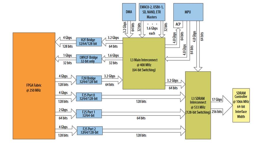
The picture shown below is the memory architecture of an Arria 10 SOC where as I used fsdram0 and fsdram2 bus with width of 128bit(port configuration 3)
I am supplying on fsdram0 bus using msgdma st-to-mm based ip config and all the configurations for both mentioned above tests are same where as only difference is fpga fabric clock supplied for the entire process is 100MHz and 200MHz respectively.
I checked the reports of Generate HDL also as I am using f_user_clk of mpu itself which is successfully generating 200MHz clock when changed the clock settings.
My Major doubt is,
Is it suppose to happen like that?
If not then where should I correct it to get the speed/throughput double the speed than I am getting now.
- Tags:
- ddr3
- FPGA SoC And CPLD Boards And Kits
- hps
- Intel® Arria® 10 FPGAs
- Intel® QuickPath Interconnect
- Memory
Link Copied
- Mark as New
- Bookmark
- Subscribe
- Mute
- Subscribe to RSS Feed
- Permalink
- Report Inappropriate Content
HI,
Sorry. I am confused on your calculation.
In theory, DDR3 or DDR4 BW can be calculated using below formula.
DDR3/DDR4 BW = operating freq (MHz) x 2 x DQ data width
From your diagram, I can see that the theoretical BW will be 1066MHz x 2 x 64 ~ 17GBps
Adjusting FPGA core clock frequency will only affect the speed where user transfer data to DDR3/DDR4 IP but it will not change the BW of the DDR3/DDR4 IP unless you change the operating frequency or DQ data width.
Thanks.
Regards,
dlim
- Mark as New
- Bookmark
- Subscribe
- Mute
- Subscribe to RSS Feed
- Permalink
- Report Inappropriate Content
Yeah I also mean that only when I changed Fpga core clock from 100MHz to 200MHz I should suppose to see double the rate of 8.88Gbps which I was getting previously why because DDR3 I have configured is for 600MHz for 32 DQ bits i.e.., 600MHz*2*32 = 37.5Gbps.
Where as through fsdram0 bus when I connected for 100MHz also I see same 8.88Gbps and for 200MHz also I see same 8.88Gbps which is very strange.
- Mark as New
- Bookmark
- Subscribe
- Mute
- Subscribe to RSS Feed
- Permalink
- Report Inappropriate Content
Sorry, I still don't quite get your question here.
May I know are you changing your DDR3 IP operating frequency or DQ data width ?
- If yes, then I would expect more BW transfer
- If no, then I would expect the same BW transfer
My point is changing FPGA core clock frequency won't affect the BW transfer
Thanks.
Regards,
dlim
- Mark as New
- Bookmark
- Subscribe
- Mute
- Subscribe to RSS Feed
- Permalink
- Report Inappropriate Content
May I know are you changing your DDR3 IP operating frequency or DQ data width ?
- If yes, then I would expect more BW transfer
- If no, then I would expect the same BW transfer
--> for the above question also my answer is I changed my ddr3 operating frequency also from 600MHz to 750MHz still I am getting the same bandwidth or speed of transfer.
My point is changing FPGA core clock frequency won't affect the BW transfer
--> If we change or increase FPGA core clock frequency and supply more data then why not increase in the speed of data transfer because according to all the documents or datasheets shared by intel for burst mode atleast 60% efficiency i should suppose to get if I use everything upto the max. But I am getting hardly 30% efficiency only. May I know why or what factors affects this..?
- Mark as New
- Bookmark
- Subscribe
- Mute
- Subscribe to RSS Feed
- Permalink
- Report Inappropriate Content
HI,
- Regarding changing DDR3 freq from 600MHz to 750MHz doesn't increase the BW
- Byright you should see some improvement on BW.
- Dummy question - just to ensure you also change your on board clock source to pump in the correct frequency to PLL refclk pin to boost DDR3 frequency to 750MHz, right ?
- Factor affecting the efficiency
- Your data path transfer need to pass through a lot of design block before it can reach DDR3 IP like your user logic design, dma IP, SDRAM L3 interconnect
- Any efficiency drop in any of this design block may affect your overall BW. The bottleneck can be anywhere. You can look into your design to see if you can optimize your design further.
- For DDR3 IP wise, the main factor will be refresh control and also addressing access (sequential will be better than random)
Thanks.
Regards,
dlim
- Subscribe to RSS Feed
- Mark Topic as New
- Mark Topic as Read
- Float this Topic for Current User
- Bookmark
- Subscribe
- Printer Friendly Page
