- Mark as New
- Bookmark
- Subscribe
- Mute
- Subscribe to RSS Feed
- Permalink
- Report Inappropriate Content
Hello all,
I am using an Arria 10 10AX027H4F35E3SG and have included a DDR4 EMIF. I am feeding the FPGA a 133MHz clock as the pll reference. This same clock is used for all the board interface timing.
When I compile the FPGA and try to establish timing constraints relative to this input clock, the tools won't let me. It will let me specify timing constraints relative to a clock output from the pll, but that differs from the input clock by several ns.
In the auto-generated verilog for the pll instance, it sets the compensation_mode to "emif" and I cannot find any documentation for that mode. It appears from the comments in the verilog that similar to "direct" mode, the pll does not phase the outputs to be in sync with the input clock. I could not find any option in the IP generation that would let me specify the compensation_mode of the IOPLL used in the EMIF.
What is the recommended way to constrain timing to a board clock that is used as the reference for the EMIF PLL?
Would it be safe to manually edit the pll verilog and change the compensation_mode from "emif" to "normal"?
Thanks.
Link Copied
- Mark as New
- Bookmark
- Subscribe
- Mute
- Subscribe to RSS Feed
- Permalink
- Report Inappropriate Content
Dear WKapp,
EMIF mode has been removed or no longer available from the Assignment Editor list in newer Quartus version ( for example v18.1). Hence, may I know what Quartus version are you using? I suggest you to use the latest version like 18.1.
Below is just for your information about the EMIF mode😊
- The EMIF mode should only be used by the EMIF IP. In differences perspective between the direct and EMIF mode, both are effectively the same. The different is that the VCO frequency range is slight different. And we suggest user to continue use the direct mode because as mentioned they are going to remove the EMIF mode from the list in newer version as I mentioned above.
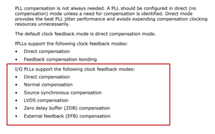
By default, the clock feedback mode is "direct" compensation mode where PLL does not compensate for any clock networks. To change the mode, you can directly change at the Assignment Editor or your verilog file and re-compile your design.
Hope this helps.
Thanks
Regards,
NAli1
- Mark as New
- Bookmark
- Subscribe
- Mute
- Subscribe to RSS Feed
- Permalink
- Report Inappropriate Content
NAli1,
Thanks for the reply. Not sure the source of your information, but my IP was generated with Quartus Prime Pro 18.1 and it has selected "emif" as the compensation_mode for the PLL. I also generated the IP with Quartus Prime Pro 19.1 and it, too, selects "emif" for the compensation_mode.
I did try to manually edit the file to select "normal", but this fails in the fitter, unable to place an auto promoted global signal from the PLL.
I would like to ask a more general type question:
When designing an FPGA such as the Arria 10 and included in the design is an EMIF such as mine, the PLL outputs the clocks that should be used for all the FPGA logic inside. Now, these PLL output clocks are not phase related to the PLL input reference clock. So, what are the best practices for interfacing the FPGA to other board elements?
In my case, I have a board clock that is used by essentially everything on the board. In a previous FPGA (a GX130), its memory controller (an ALTMEMPHY) included a PLL that operated in "normal" mode, so its output clocks were in phase with the input reference clock, and I fed that from the board clock. Now, with the Arria 10, all the interfaces that use the board clock can never be used with the FPGA io since that clock is not in phase with the FPGA fabric.
Thanks,
Bill
- Mark as New
- Bookmark
- Subscribe
- Mute
- Subscribe to RSS Feed
- Permalink
- Report Inappropriate Content
Hi WKapp,
I am sorry if I misunderstood your question. Perhaps what I replied previously is too general. Let me try to clarify again and be more specific. 😊 Let’s talk about 2 different perspective as below:
1. EMIF IP perspective:
2. General perspective ( Ex: customer own design and etc)
1. EMIF IP:
Question: What is the recommended way to constrain timing to a board clock that is used as the reference for the EMIF PLL?
Answer: For Arria 10 EMIF, the clock input pin (emif pll ref clk) is connected to dedicated clock pin thus you do not need additional constrain timing.
Question: Would it be safe to manually edit the pll verilog and change the compensation_mode from "emif" to "normal"?
Answer: I assume you are talking about EMIF IP. For EMIF, the compensation mode is already customize for that EMIF IP and it is not changeable. In short, user do not need to worry about what mode they are using because the IP will take care of it.
For more information about the PLL clock you may refer to this emif handbook à https://www.intel.com/content/dam/www/programmable/us/en/pdfs/literature/ug/ug-20115.pdf
2. General perspective ( Ex: customer own design and etc)
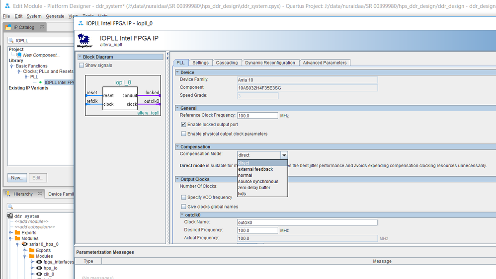
I am not sure why you still able to see the “emif” setting as at my side I am not seeing this listed (see my 2nd screenshot). Even in Arria 10 device handbook chapter 4.2.4. Clock Feedback Modes also didn’t support “emif” mode. à https://www.intel.com/content/dam/www/programmable/us/en/pdfs/literature/hb/arria-10/a10_handbook.pdf
Also another way I would recommend you change the PLL compensation mode is by generating the IOPLL from the Qsys IP with the correct compensation mode selected.
Hope this answered the questions.
Regards,
NAli1
- Mark as New
- Bookmark
- Subscribe
- Mute
- Subscribe to RSS Feed
- Permalink
- Report Inappropriate Content
NAli1,
I am sorry if I am not stating my question properly, I do not think you understand what I am asking. So, I will try to ask more clearly with the help of a picture.
Question: What is the recommended way to constrain timing to a board clock that is used as the reference for the EMIF PLL?
Answer: For Arria 10 EMIF, the clock input pin (emif pll ref clk) is connected to dedicated clock pin thus you do not need additional constrain timing.
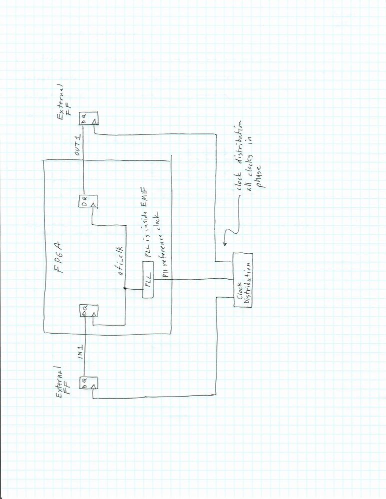
I understand that the memory timing is all constrained, and in my design the memory portion meets timing. My question is not about the memory timing, it is about timing of other FPGA elements. Please look at the following picture (sorry it is rotated):
First of all, the clock distribution on the board guarantees that all the clocks are in phase at their destinations. For the purpose of this analysis, please assume the skew between clocks is 0.
I have shown 1 input to the FPGA and 1 output from the FPGA, both are connected to external FFs. The board clock that connects to the FFs is the same clock used as the PLL reference clock input. The PLL shown inside the FPGA is the one instantiated as part of the EMIF, and one of its output clocks is used inside the FPGA to clock all the fabric.
My problem is that the since the PLL has compenstation_mode = "emif", there is no guaranteed phase relationship between the PLL reference clock input (board clock) and the internal FPGA clock (afi_clk). I want to specify timing constraints for the inputs and outputs relative to the board clock but cannot since there is no known phase relationship.
I originally thought I could change the mode of the PLL manually to "normal". If I could, this would make afi_clk in phase with the PLL reference clock, and I could use the PLL reference clock in my timing constraints. However, I cannot set the mode to "normal". It appears that "emif" mode is similar to "direct" mode in that it does not care about the phase.
I hope the above is clear.
So, please explain, how do I create timing constraints for my example input and output?
Thanks,
Bill
- Mark as New
- Bookmark
- Subscribe
- Mute
- Subscribe to RSS Feed
- Permalink
- Report Inappropriate Content
Hi WKapp,
Sorry for the delay in response because we are on long holiday in my region.
For the EMIF IP, it should connect to DDR4 module, but we don see DDR4 in the diagram.
If I assume the "FF" is referring to DDR4 module, we don't need connect clock to the DDR4 externally. The clock to DDR4 module is supply from FPGA<-->DDR4 interface.
Thanks
Regards,
NAli1
- Mark as New
- Bookmark
- Subscribe
- Mute
- Subscribe to RSS Feed
- Permalink
- Report Inappropriate Content
- Mark as New
- Bookmark
- Subscribe
- Mute
- Subscribe to RSS Feed
- Permalink
- Report Inappropriate Content
Dear WKapp,
I really thank you for your detail explanation and now I think I understand your issue better. 😊
You are trying to constraint timing for other logic (IN1 and OUT1) and not the EMIF as the EMIF don’t need the additional timing constraint as per I explained before.
And from the diagram you attached, I can see that you are using the afi_clk to drive non-EMIF logic. As far as I know, there are no afi_clk exported from EMIF IP unless you are using “Hard PHY only” mode. Are you using “Hard PHY only” mode?
This afi_clk is actually meant for the custom controller to use and not for other logic like External FF.
Anyway, here is some constraint guideline that I hope is helpful for you to get some idea on how to constraint timing --> https://www.intel.com/content/dam/www/programmable/us/en/pdfs/literature/manual/mnl_timequest_cookbook.pdf
I believed the problem you are facing now is more to timing issue and not EMIF. My suggestion to you is to open new thread if you encounter any issue from the documentation and Timing expert will help you.
Thanks
Regards,
NAli1
- Mark as New
- Bookmark
- Subscribe
- Mute
- Subscribe to RSS Feed
- Permalink
- Report Inappropriate Content
- Mark as New
- Bookmark
- Subscribe
- Mute
- Subscribe to RSS Feed
- Permalink
- Report Inappropriate Content
Hi WKapp,
I consult timing expert guy, and he also aware about the difficultly in meeting timing based on your situation as the clock is not in the same phase.
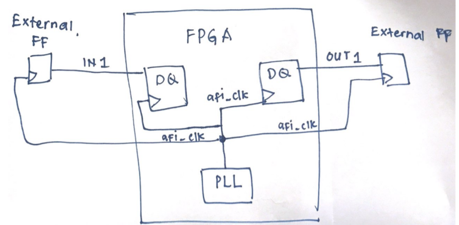
His recommendation for you is to connect the afi_clk out externally to your External FF instead of using clock distribution so that all the clock will have same source be in same phase.
I attached diagram for your reference.
Hope this helps.
Thanks
Regards,
NAli1
- Mark as New
- Bookmark
- Subscribe
- Mute
- Subscribe to RSS Feed
- Permalink
- Report Inappropriate Content
- Mark as New
- Bookmark
- Subscribe
- Mute
- Subscribe to RSS Feed
- Permalink
- Report Inappropriate Content
Dear WKapp,
Understand the pain that you are facing. I sincerely apologize for the inconvenience caused.
Regards,
NAli1
- Mark as New
- Bookmark
- Subscribe
- Mute
- Subscribe to RSS Feed
- Permalink
- Report Inappropriate Content
- Subscribe to RSS Feed
- Mark Topic as New
- Mark Topic as Read
- Float this Topic for Current User
- Bookmark
- Subscribe
- Printer Friendly Page


