- Mark as New
- Bookmark
- Subscribe
- Mute
- Subscribe to RSS Feed
- Permalink
- Report Inappropriate Content
Hello,
I am working on a project where I use:
1) 1-port (or 2-port) on-chip RAM (Block RAM) with data width 128b and size of 360960B, running at 160MHz.
2) A process for capturing camera data (DCMI interface) running at 26.67MHz and storing 752x480 monochrome images into the BRAM (by 16px chunks, when needed) using the port A.
3) A process for VGA output (to HDMI transceiver ADV7513 on DE10-Nano) running at 40MHz, loading the image by 16px chunks from the BRAM (when needed) using the port B.
4) Clock 160MHz is generated by PLL from the 50MHz input clock, frequencies 40MHz (160/4) and 26.67MHz (160/6) are generated from the 160MHz using second PLL.
Everything works fine both with the built-in 1-port RAM (Altera Megafunction IP) and with custom inferred 2-port BRAM (using this VHDL code). (I don't use Altera's 2-port RAM because I was not able to get it working with SignalTap, which was complaining about size limit of 553 blocks.)
The SignalTap recording of the ports of the custom 2-port BRAM is in the next image:
And the resulting image on the HDMI output looks as expected:
Because I would like to use also HPS, I tried to add soc_system.qip generated by the Platform Designer. I used the working DDR configuration from the GHRD, removed all GPIOs, peripherals, kept only Clock source IP component (connected to the 50MHz clock) and the HPS IP block to have a minimal configuration of the HPS.
But for some reason when the soc_system component in the top module is initialized, the BlockRAM read (dout) port starts behaving weird (even it is completely separate from the soc_system component):
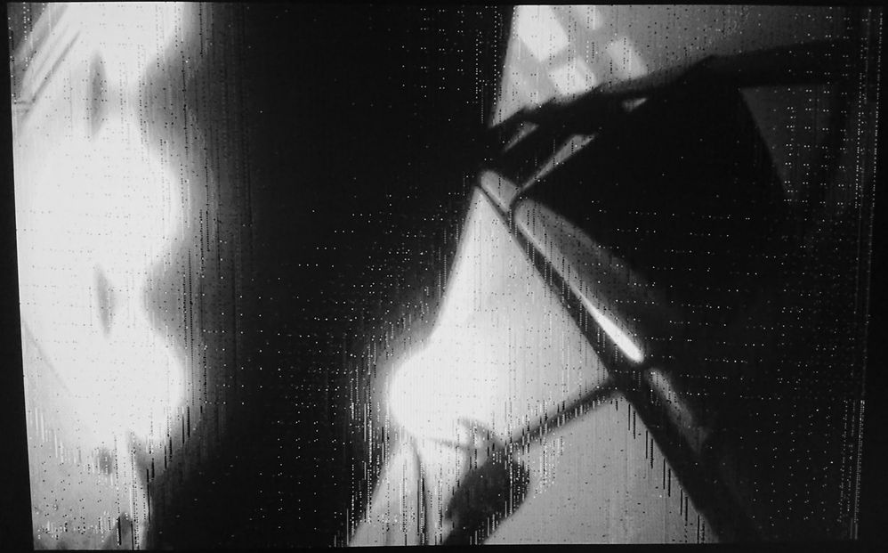
And it results in the following artifacts in the HDMI output:
I really don't understand why this is happening. I tried to feed the clock source with the derived 40MHz clock (I thought it could be a timing issue) but it behaves the same. The same problem happens with the Altera's 1-port RAM. When I comment out the system_soc component and remove the qip file from the project, it starts working correctly again..
Thanks for any suggestions on what I am doing wrong and how this can be solved.
Link Copied
- Mark as New
- Bookmark
- Subscribe
- Mute
- Subscribe to RSS Feed
- Permalink
- Report Inappropriate Content
HI,
May I know which GHRD design are you referring too?
I am intrigues why you wanna use HPS
Is the timing clean? setup, hold etc?
Is it possible to attach the design or internally send me the qar for investigation to narrow down the issue.
- Mark as New
- Bookmark
- Subscribe
- Mute
- Subscribe to RSS Feed
- Permalink
- Report Inappropriate Content
Hi,
I am referring to DE10_NANO_SoC_GHRD from the DE10-Nano_v.1.3.8_HWrevC_SystemCD. To be specific I took the important settings and the pin assignments from the GHRD project to my own project.
I currently use the HPS only for camera initialization over I2C (of course this could be done in the fabric directly as I do it for the ADV7513 chip on-board). But I am planning to use the HPS to load camera recordings from the SD card to the DDR memory and load it to the BRAM from there instead of using the DCMI interface when needed (possibly using the DMA controller).
In the last experiment I used Altera's 1-port Megafunction RAM IP (entity bram0_128) with a process splitting the 1 RW port to separate read and write ports and remembering pending reads/writes. I have managed to record the HDMI output together with SignalTap (triggered on read request): here is the video with the HPS enabled and here is the video without the HPS (soc_system commented out and qip removed from the project files). I used button to increment additional hold cycles (cycles when the port splitting process waits until READ_DONE and WRITE_DONE are set), in the video there is also MEM_STATE (0=idle,1=reading,2=reading_end,3=writing) of that process, bram0_128 signals and the splitted read (running at 40MHz) and write (running at 26.67MHz) signals. Clearly there must be always at least 1 hold cycle.
I can send you the current version of the Quartus project, but without the camera board you probably won't be able to reproduce the results. Also, when the DCMI process is commented out and the VGA process reads static content of the 1-port memory (preloaded with single frame from MIF) then the problem disappears (with HPS enabled). Not sure why.
Thanks for your support!
EDIT: For completeness here is a video with 2-port BRAM (port A used for writing used by DCMI process with WREN always high), trigger at write address = 0001, without RDEN (always 1).
EDIT 2: There must be something terribly wrong with the HPS or with the project settings. The MEM_STATE signal defined as 2-bit STD_LOGIC_VECTOR representing all 4 possible states of BRAM accessing process sometimes unexpectedly changes to wrong state. When I used states defined as TYPE state IS (S0, S1, S2, S3) which are compiled into 4 STD_LOGIC wires and there should always be 1 of the wires active at one moment, then with the system_soc active in the project all of them suddenly were 0 from one point (so it was impossible to handle that state in VHDL) and the whole process stopped working..
EDIT 3: I decided to share the project here, qar file is attached.
- Mark as New
- Bookmark
- Subscribe
- Mute
- Subscribe to RSS Feed
- Permalink
- Report Inappropriate Content
Hello,
I am escalating this to soc SME, thus you will expect a response soon.
- Mark as New
- Bookmark
- Subscribe
- Mute
- Subscribe to RSS Feed
- Permalink
- Report Inappropriate Content
Hi vrbavojtech,
Sorry for late reply. I was trying to find if there was any similar cases before.
Is it possible to try using a GHRD/GSRD to start build your system before any additional functional features added on?
https://releases.rocketboards.org/
Thanks.
Regards,
Aik Eu
- Mark as New
- Bookmark
- Subscribe
- Mute
- Subscribe to RSS Feed
- Permalink
- Report Inappropriate Content
Hi vrbavojtech,
I am thinking it will be more easy to troubleshoot the problem if using a default working soc system design before making further changes.
Thanks.
Regards,
Aik Eu
- Mark as New
- Bookmark
- Subscribe
- Mute
- Subscribe to RSS Feed
- Permalink
- Report Inappropriate Content
Hi vrbavojtech,
FYI. You can refer to this document for your reference related to HDMI hardware design, I think it may help to troubleshoot or as a comparison to identify some of the design related problems:
Thanks.
Regards,
Aik Eu
- Mark as New
- Bookmark
- Subscribe
- Mute
- Subscribe to RSS Feed
- Permalink
- Report Inappropriate Content
- Mark as New
- Bookmark
- Subscribe
- Mute
- Subscribe to RSS Feed
- Permalink
- Report Inappropriate Content
Hi vrbavojtech,
As we do not receive any response from you on the previous question/reply/answer that we have provided. Please login to ‘https://supporttickets.intel.com’, view details of the desire request, and post a feed/response within the next 15 days to allow me to continue to support you. After 15 days, this thread will be transitioned to community support. The community users will be able to help you on your follow-up questions.
Thanks.
Regards,
Aik Eu
- Mark as New
- Bookmark
- Subscribe
- Mute
- Subscribe to RSS Feed
- Permalink
- Report Inappropriate Content
Hi,
I believe I have already solved this problem. It was caused by wrong timing constraints in the SDC file for the HDMI and DCMI interfaces, I also didn't know it has to be added to the file list in Quartus otherwise it gets ignored completely by the Fitter during project compilation.
Sometimes the image glitches again, eg. when I add some VHDL signal accessed by a VHDL process serving the VGA output and also by another process sensitive to an edge of a different clock signal - I am still not sure why this interconnecting signal breaks it, so I just have to be careful about using the signals "properly". Sometimes the glitch happens even when I make minor changes to VGA-unrelated processes, also not sure why.
Thanks anyway.
- Subscribe to RSS Feed
- Mark Topic as New
- Mark Topic as Read
- Float this Topic for Current User
- Bookmark
- Subscribe
- Printer Friendly Page


