- Mark as New
- Bookmark
- Subscribe
- Mute
- Subscribe to RSS Feed
- Permalink
- Report Inappropriate Content
Dear Support/Expert,
While I am leaning how to compile a DDR4 with Quartus Pro.
I got a message
Error(175011): Conflicting region assignments found for DQ_GRP, which is within External Memory Interfaces Intel Arria 10 FPGA IP jesd204b_emif_0_altera_emif_1920_n6nqnfq.
After I comment out most of the pin assignment, I find the problem is
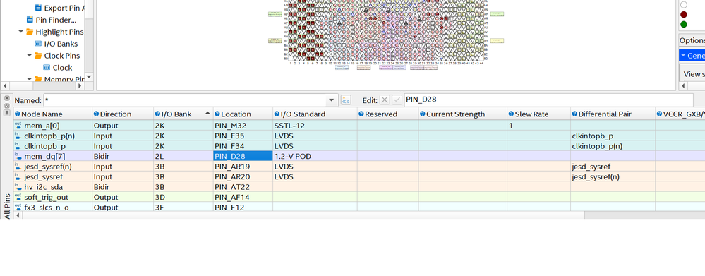
set_location_assignment PIN_D28 -to mem_dq[7].
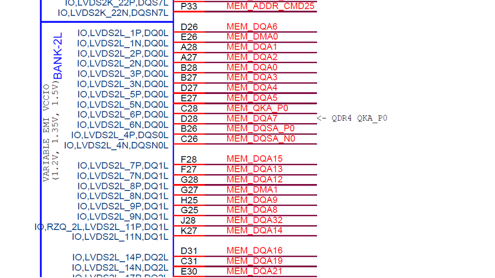
on the Arria 10X dev board, the Mem_dq[7] must be on D28.
and it is the only pin on bank 2L. I don't know what I can do to over come this problem.
Please give me some suggestion. appreciate your help.
David
- Mark as New
- Bookmark
- Subscribe
- Mute
- Subscribe to RSS Feed
- Permalink
- Report Inappropriate Content
Hi David,
I can see the alert_n pin that you disabled.
Actually the alert_n pin configuration is in the EMIF IP.
When you open the EMIF IP in IP Parameter Editor, under the Memory tab, in Topology section, there is a ALERT# pin placement option.
The EMIF IP will reserve the location that you have set for the alert_n pin.
In your project, I can see that you set it to I/O Lane with DQS Group 0.
So the pin location should be in the Bank 2L where there is your DQS Group 0 - 3.
Because the alert_n pin is not been set by the user, the Quartus will set it for you.
In this case, I can see that the Quartus has set it to pin C28.
So now you can change the pin location from E35 to C28 or just let the Quartus set it for you.
I generate the .tcl file from the Pin Planner in case you want to refer the pin location that have been changed.
But I also share the .qsf file to ease your work.
Don't worry on how to use it.
It's just for reference purpose.
I'm sorry for confusing you.
Please let me know if you're still having trouble with it.
Thanks,
Adzim
Link Copied
- Mark as New
- Bookmark
- Subscribe
- Mute
- Subscribe to RSS Feed
- Permalink
- Report Inappropriate Content
Hi David,
May I have your design for me to replicate the error?
Thanks,
Adzim
- Mark as New
- Bookmark
- Subscribe
- Mute
- Subscribe to RSS Feed
- Permalink
- Report Inappropriate Content
Hi Adzim
Thank you so much if you can give me some deep help. this is a demo project that shows how to collect data through JESD204B. original project is on 10AX115H2F34E1SG(Standard version 15.1.0). My goal is to port it to Intel GX dev board. 10AX115S2F45I1SG. I have two major tasks, first is the original design was not based on Hilo memory card, so I need mapping the pins from original pin name to Intel Dev board. ( there is a mapping chart in the Intel released schematic, but I am not 100% sure I did it correct, because I don't have a Hilo memory card schematic). Second is the tooling upgrade. I don't really mind it is a standard version or pro, as I got a Pro License with the Dev Kits, so better to use Pro.
I have been doing the logic/circuit design for a long time, but not very familiar with the Platform Designer and Arria 10 family. I don't have a clear route to trouble shoot this compilation fail problem, I have watched few training video, and browsed some user guide. because of the short time, I haven't figure out a way to do this.
I attached a .qar file. even I commented out few pin assignment which will fail the fitter, it still failed fitter, the assignments are required by the Hilo DDR4 memory card, so location should not be changed.
Appreciate your help
David
- Mark as New
- Bookmark
- Subscribe
- Mute
- Subscribe to RSS Feed
- Permalink
- Report Inappropriate Content
this is the original qar file.
- Mark as New
- Bookmark
- Subscribe
- Mute
- Subscribe to RSS Feed
- Permalink
- Report Inappropriate Content
Hi David,
Thanks for sharing the qar file and the information regarding to problem.
I need some time to work on this.
I will feedback to you later.
But may I know which Quartus Pro version that you used?
Thanks,
Adzim
- Mark as New
- Bookmark
- Subscribe
- Mute
- Subscribe to RSS Feed
- Permalink
- Report Inappropriate Content
Hi Adzim
I am using the 21.3.0 Pro. the original design is 64 bits DDR4, but not Hilo formfactor, so besides I did an auto IP upgrade for all IPs, I manually generate the Quartus provided example Hilo IP for Arria 10 GX dev board. and modified it from 72 bits to 64 bits. I am not sure I did it correctly, but it will compile without the pin assignment, once I assign the pin following the Dev board schematic, then the Quartus will report resource conflict. I don't know how to over come the gap between the two EMIF IP.
Thank you,
David
- Mark as New
- Bookmark
- Subscribe
- Mute
- Subscribe to RSS Feed
- Permalink
- Report Inappropriate Content
Hi David,
I can compile the project successfully by relocating the pin locations in DQ Group.
I can see that the pins have been assigned to wrong group which cause the errors.
I've reassigned all mem_dbi_n pins to the right location.
I also have assigned the location for dqs pins and some dq pins which are missing and misplace in the wrong Bank.
I've attached the tcl file from the pin planner and qsf file for your reference.
Please let me know if you're facing some problems with it.
Thanks,
Adzim
- Mark as New
- Bookmark
- Subscribe
- Mute
- Subscribe to RSS Feed
- Permalink
- Report Inappropriate Content
Hi Adzim
I am very grateful for the detailed touch of my project, it is a miracle, it would take me weeks to figure this out. this is called support instead of like other people told me to read the manual or take the training.
there are still two things, one is directly related one is for basic knowledge suggestion.
for the qsf file, this is still one line that I commented which should be enabled.
#set_location_assignment PIN_E35 -to mem_alert_n[0].
I don't really know that is mem_alert_n[0] for. but it ME_ADDR_CMD[29] (N4 Pin on the Hilo memory slot). once uncomment this line, the compilation will fail again, why by adding just one more pin will fail the compilation.
Info(14710): The I/O pad mem_dqs[0] is constrained due to: User Location Constraints (PIN_B26)
Info(14710): The I/O pad mem_alert_n[0] is constrained due to: User Location Constraints (PIN_E35)
Error(14566): The Fitter cannot place 1 periphery component(s) due to conflicts with existing constraints . Fix the errors described in the submessages, and then rerun the Fitter. The Intel FPGA Knowledge Database may also contain articles with information on how to resolve this periphery placement failure. Review the errors and then visit the Knowledge Database at https://www.altera.com/support/support-resources/knowledge-base/search.html and search for this specific error message number.
Error(175011): Conflicting region assignments found for DQ_GRP, which is within External Memory Interfaces Intel Arria 10 FPGA IP jesd204b_emif_0_altera_emif_1920_n6nqnfq
Info(175028): The DQ_GRP name(s): jesd204b_inst|emif_0|emif_0|arch|arch_inst|io_tiles_wrap_inst|io_tiles_inst|tile_gen[0].lane_gen[0].lane_inst_DQ_GRP_1
Info(175014): Component must be in region from (78, 196) to (78, 207) due to the following assignment(s)
Info(14710): The I/O pad mem_dqs[0] is constrained due to: User Location Constraints (PIN_B26)
Info(175014): Component must be in region from (78, 169) to (78, 180) due to the following assignment(s)
Info(14710): The I/O pad mem_alert_n[0] is constrained due to: User Location Constraints (PIN_E35)
Info(14709): Each constrained I/O pad is contained within this DQ_GRP
Info(175028): The DQ_GRP name(s): jesd204b_inst|emif_0|emif_0|arch|arch_inst|io_tiles_wrap_inst|io_tiles_inst|tile_gen[0].lane_gen[0].lane_inst_DQ_GRP_1
Info(175014): Component must be in region from (78, 196) to (78, 207) due to the following assignment(s)
Info(14710): The I/O pad mem_dqs[0] is constrained due to: User Location Constraints (PIN_B26)
Info(175014): Component must be in region from (78, 169) to (78, 180) due to the following assignment(s)
Info(14710): The I/O pad mem_alert_n[0] is constrained due to: User Location Constraints (PIN_E35)
---------------------------------------------------------
second question is more generic, I don't know how to use the .TCL file. during the training I know in the command window, by running TCL script, I can run some complicate simulation. in this case, how can I use this TCL file, you can just give a link of the TCL tutorial, I need learn this section carefully.
Best Regards,
David
- Mark as New
- Bookmark
- Subscribe
- Mute
- Subscribe to RSS Feed
- Permalink
- Report Inappropriate Content
Hi David,
I can see the alert_n pin that you disabled.
Actually the alert_n pin configuration is in the EMIF IP.
When you open the EMIF IP in IP Parameter Editor, under the Memory tab, in Topology section, there is a ALERT# pin placement option.
The EMIF IP will reserve the location that you have set for the alert_n pin.
In your project, I can see that you set it to I/O Lane with DQS Group 0.
So the pin location should be in the Bank 2L where there is your DQS Group 0 - 3.
Because the alert_n pin is not been set by the user, the Quartus will set it for you.
In this case, I can see that the Quartus has set it to pin C28.
So now you can change the pin location from E35 to C28 or just let the Quartus set it for you.
I generate the .tcl file from the Pin Planner in case you want to refer the pin location that have been changed.
But I also share the .qsf file to ease your work.
Don't worry on how to use it.
It's just for reference purpose.
I'm sorry for confusing you.
Please let me know if you're still having trouble with it.
Thanks,
Adzim
- Mark as New
- Bookmark
- Subscribe
- Mute
- Subscribe to RSS Feed
- Permalink
- Report Inappropriate Content
Hi Adzim
Thank you again for the helping. I guess this is not a critical signal, so I can temporary commented it out and going forward. but I did play with the IP for a while, and here is the observation. I created a new example from scratch using 10AX DEv board example. by default the mem_alert_n was assigned to Pin_E35. and the example couldn't compile by default. the error message is very similar to the one that I have. see attached the qar file, and the error message I copied during the compilation. I am new and don't fully understand what does it mean like
Info(175014): Component must be in region from (78, 196) to (78, 207) due to the following assignment(s).
once I comment mem_alert_n at Pin_E35, everything will compile successful.
I guess there may be some tricky stuff not special to my project.
again, I am very grateful to your in-depth help. and in short term I believe I will post a lot question on the forum. hope continuously to get your support.
Best Regards,
David
- Mark as New
- Bookmark
- Subscribe
- Mute
- Subscribe to RSS Feed
- Permalink
- Report Inappropriate Content
Hi David,
I think that the ALERT pin is special pin for the DDR4 interface.
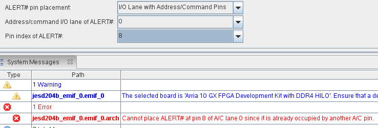
Even if the pin is not assigned by the user, the pin will be assigned by the Quartus as shown in image below.
The Quartus will fit the location for the signal for you.
If you want to use the pin E35, you must change the setting in EMIF IP for ALERT pin location.
As you can in the image below, the setting is set to Address/Command lane 0 with pin no. 8.
This location is also same as pin E35.
But the location is already been used by other signal.
So the ALERT pin location will be determined in this EMIF IP setting and you should aware of where you should assign the pin.
Thanks for posting your question in Intel Community.
Regards,
Adzim
- Mark as New
- Bookmark
- Subscribe
- Mute
- Subscribe to RSS Feed
- Permalink
- Report Inappropriate Content
Hi Adzim,
on the Intel A10 GX dev board, the ALERT pin from Hilo memory card is physically connected to Arria 10 Pin E35. so I don't think use other pins is an option.
I create a new IP from scratch by using presets for emif_0 Arria 10 GX FPGA Development Kit with DDR4 HILO. there should not have any other assignment.
why it report
Error: emif_0.arch: Cannot place ALERT# at pin 8 of A/C lane 0 since it is already occupied by another A/C pin.
to isolate the possible wrong assignment or resource conflict in my project. why the original Intel preset IP still have the Alter# error. I think alter# has to be assigned to E35.
thank you,
David
- Mark as New
- Bookmark
- Subscribe
- Mute
- Subscribe to RSS Feed
- Permalink
- Report Inappropriate Content
Hi Adzim
After I played with the Platform Designer, I think I figured out my problem, if I create an example from original 72 bit IP. everything is OK, the pin will be put on the E35 by default, and compile no problem, but when I change it to 64 bits( because the original design from Texas Instrument is 64 bits). then the Platform Designer will complain that
Error: emif_0: "DQS group of ALERT#" (MEM_DDR4_ALERT_N_DQS_GROUP) 8 is out of range: 0, 1, 2, 3, 4, 5, 6, 7
it is reasonable to remove the 9th group. but I guess the Alert# is bundled with this DQS group 8 is the one that connected to the E35.
That is my problem, If to fix from the Platform Designer side is too complicated. I will instantiate a 72 bit emif bus, and from the project level, unconnect (disable) the top 8 bits. hope it will work.
thank you for help.
David
- Mark as New
- Bookmark
- Subscribe
- Mute
- Subscribe to RSS Feed
- Permalink
- Report Inappropriate Content
Hi Adzim,
Now I have another headache. the whole project I am porting to the Intel A10 GX dev board is based on 64 bit DDR4.
if I use the preset DDR4 HiLO 72 bits, then I have to change all the MM bus of the project from 512 to 576( DDR X 8).
if I change preset DDR4 HiLO to 64 bits, then the Alert# won't be able to assign to Pin_E35. I am not that familiar with the DDR4 standard, is this Alert# very critical? can I ignore it when prototype with the Dev Kit, and make the fix in the final production board design?
thank you,
David
- Mark as New
- Bookmark
- Subscribe
- Mute
- Subscribe to RSS Feed
- Permalink
- Report Inappropriate Content
Hi David,
I'm really sorry because it's my fault to judge the pin location for pin E35.
The pin E35 is not in lane 0 index 8, but it is in lane 3 index 0.
I've referred to the Arria 10 Pin-Out file to confirm the pin location.
I also have applied the changes into your project and it's working.
Here are some steps that you can follow:
-
Change the following setting: (The changes is in EMIF IP in the Memory tab under the Topology section)
-
ALERT# pin placement: I/O Lane with Address/Command Pins
-
Address/command I/O lane of ALERT#: 3
-
Pin index of ALERT#: 0
-
-
Save and regenerate your EMIF IP.
-
Enable the mem_alert_n pin location to pin E35. (if you enable it through .qsf file, you need to restart the Quartus software)
-
Compile the project.
I hope you're able to make it from your site.
Please let me know if you still need help on this.
Regards,
Adzim
- Mark as New
- Bookmark
- Subscribe
- Mute
- Subscribe to RSS Feed
- Permalink
- Report Inappropriate Content
Hi Adzim
It works now, thank you very much.
David
- Subscribe to RSS Feed
- Mark Topic as New
- Mark Topic as Read
- Float this Topic for Current User
- Bookmark
- Subscribe
- Printer Friendly Page


