- Mark as New
- Bookmark
- Subscribe
- Mute
- Subscribe to RSS Feed
- Permalink
- Report Inappropriate Content
Hi,
I am trying to read/write from/to an external memory model during the simulation using EMIF.
I have some questions regarding the address map in EMIF.
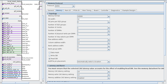
Based on this configuration, what should be the address width? I guess it should be 29 bits, right?
But, why the amm_address is 26 bits here?
Also, I can't understand why mem_a is 17 bits.
The other problem is that I don't know how to generate certain addresses if I want to read or write from/to memory. What is the meaning of each bit of this 26-bit amm_address?
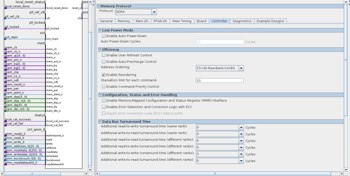
Here is the Controller configuration:
Thank,
-- Mahdi
- Mark as New
- Bookmark
- Subscribe
- Mute
- Subscribe to RSS Feed
- Permalink
- Report Inappropriate Content
For the address ordering that you used:
CS-CID-Row-Bank-Column-BG
The CS is available only when there is multiple rank.
The CID is for 3D stacked interface. No CID bit in this configuration.
Row address width = 15.
Column address width = 10.***
Bank address width = 2.
Bank group width = 2.
***(Lower 3 bits has been set to 0 because Avalon bus is 8x wider than EMIF bus in Quarter rate. Therefore it's removed when mapping to Avalon address)
The ordering will be as below:
Row[14..0] = amm_address[25..11]
Bank[1..0] = amm_address[10..9]
Column[9..3] = amm_address[8..2]
BG[1..0] = amm_address[1..0]
Link Copied
- Mark as New
- Bookmark
- Subscribe
- Mute
- Subscribe to RSS Feed
- Permalink
- Report Inappropriate Content
Hi Mahdi,
Thank you for submitting your question in Intel Community.
I'm Adzim, application engineer will assist you in this thread.
In my opinion, you need to refer to memory datasheet for the truth table of the memory commands.
Cheers,
Adzim
- Mark as New
- Bookmark
- Subscribe
- Mute
- Subscribe to RSS Feed
- Permalink
- Report Inappropriate Content
Hi Adzim,
Thanks for your reply. I am not using the actual memory system. I am using the memory IP core that is generated in EMIF design example, and I do not know its specifications.
- Mahdi
- Mark as New
- Bookmark
- Subscribe
- Mute
- Subscribe to RSS Feed
- Permalink
- Report Inappropriate Content
For the address ordering that you used:
CS-CID-Row-Bank-Column-BG
The CS is available only when there is multiple rank.
The CID is for 3D stacked interface. No CID bit in this configuration.
Row address width = 15.
Column address width = 10.***
Bank address width = 2.
Bank group width = 2.
***(Lower 3 bits has been set to 0 because Avalon bus is 8x wider than EMIF bus in Quarter rate. Therefore it's removed when mapping to Avalon address)
The ordering will be as below:
Row[14..0] = amm_address[25..11]
Bank[1..0] = amm_address[10..9]
Column[9..3] = amm_address[8..2]
BG[1..0] = amm_address[1..0]
- Mark as New
- Bookmark
- Subscribe
- Mute
- Subscribe to RSS Feed
- Permalink
- Report Inappropriate Content
Oh, I see. I did not know this fact. Thank you so much for your explanation.
- Mahdi
- Mark as New
- Bookmark
- Subscribe
- Mute
- Subscribe to RSS Feed
- Permalink
- Report Inappropriate Content
I’m glad that your question has been addressed, I now transition this thread to community support. If you have a new question, feel free to open a new thread to get the support from Intel experts. Otherwise, the community users will continue to help you on this thread. Thank you.
- Subscribe to RSS Feed
- Mark Topic as New
- Mark Topic as Read
- Float this Topic for Current User
- Bookmark
- Subscribe
- Printer Friendly Page

