Design Example - PHY Interface for PCI Express (PIPE)
Success! Subscription added.
Success! Subscription removed.
Sorry, you must verify to complete this action. Please click the verification link in your email. You may re-send via your profile.
- Intel Community
- Intel Community Knowledge Base
- Product Support Forums Knowledge Base
- FPGA Knowledge Base
- FPGA Wiki
- Design Example - PHY Interface for PCI Express (PIPE)
Design Example - PHY Interface for PCI Express (PIPE)
- Subscribe to RSS Feed
- Mark as New
- Mark as Read
- Bookmark
- Subscribe
- Printer Friendly Page
- Report Inappropriate Content
Design Example - PHY Interface for PCI Express (PIPE)
Overview
This article covers the steps required to succesfully instantiate the Phyical Layer (Gen 1 or Gen 2) of a PCIe Transceiver, including the PHY Interface for PCI Express (PIPE), on a Stratix V FPGA (For Quartus II v11.0 or v12.0sp2). It will be useful for users who want to quickly get a working PHY IP design up and running to view simulation results. The goal of the article is to briefly guide the user through the design, compilation, and simulation of the Altera generated PIPE reference design. After finishing the article, the reader will be able to:
- Identify major functional blocks within the PIPE design
- Understand at a high level the operation of the Altera generated PIPE example
- Compile the reference design in Quartus and ModelSim
- Simulate the design in ModelSim
This guide assumes the reader has standard knowledge of the use of Quartus and ModelSim.
For a general guide for designing a Trasnceiver using Altera Generated IP, see theTransceiver Design Flow Series.
External Links
V-Series Transceiver PHY IP Core User Guide) - This document describes configuration details for the PIPE (Useful when generating the IP from the MegaWizard)
V-Series Transceiver PHY IP Core User Guide - Transceiver Architecture, Clocking, Configurations and reset controller information.
Altera Avalon Memory-Mapped Interface Specification (PDF) - Avalon Mmemory-Mapped Interface Protocol information.
ModelSim SE Command Reference (PDF) - A guide to tcl commands and in ModelSim.
Design File
Quartus v11.0 b157 Altera PCIE PIPE Design File (ZIP)
Quartus v12.0 b232 Altera PCIE PIPE Design File (ZIP) (Up-to-date) Contains everything you need to compile and simulate.
Quartus v13.1 b162 Altera PCIE PIPE Design File (ZIP)
Design Specifications
The table below lists the specifications for the Quartus version 11.0 build 157 design:
| Attribute | Specification |
| Device Family | Stratix V GX |
| FPGA | 5SGXMA7K2F40C2 |
| Quartus version | QuartusII v11.0, b157 |
| Modelsim version | Modelsim SE v6.6d |
| Datarate | 5Gbps |
| Data pattern | PRBS 23 |
| Number of channels | 4 |
| IP used | PCIE PIPE PHY IP, Traceiver Reconfiguration Controller |
The table below lists the specifications for the Quartus version 12.0sp1 build 232 design:
| Attribute | Specification |
| Device Family | Stratix V GT |
| Quartus version | QuartusII v12.0, b232 |
| Modelsim version | Modelsim SE v10.0d |
| Datarate | 5Gbps |
| Data pattern | PRBS 23 |
| Number of channels | 4 |
| IP used | PCIE PIPE PHY IP, Traceiver Reconfiguration Controller |
The table below lists the specifications for the Quartus version 13.1 build 162 design:
| Attribute | Specification |
| Device Family | Stratix V GX |
| FPGA | 5SGXMA7K2F40C2 |
| Quartus version | QuartusII v13.1, b162 |
| Modelsim version | Modelsim SE v10.0d |
| Datarate | 5Gbps |
| Data pattern | PRBS 23 |
| Number of channels | 4 |
| IP used | PCIE PIPE PHY IP, Traceiver Reconfiguration Controller |
Design Overview
The design implements the following blocks:
- pcie_pipe_phy_ip (Altera Generated)
- top_reconfig (Altera Generated)
- pipe_state_mc (User Generated)
- datagen_ctrl_top (User Generated)
- datagen_16bit_top (User Generated)
- prbs_generator (User Generated)
- prbs_checker (User Generated)
- mgmt_master (User Generated)
- a transmit logic multiplexor (User Generated)
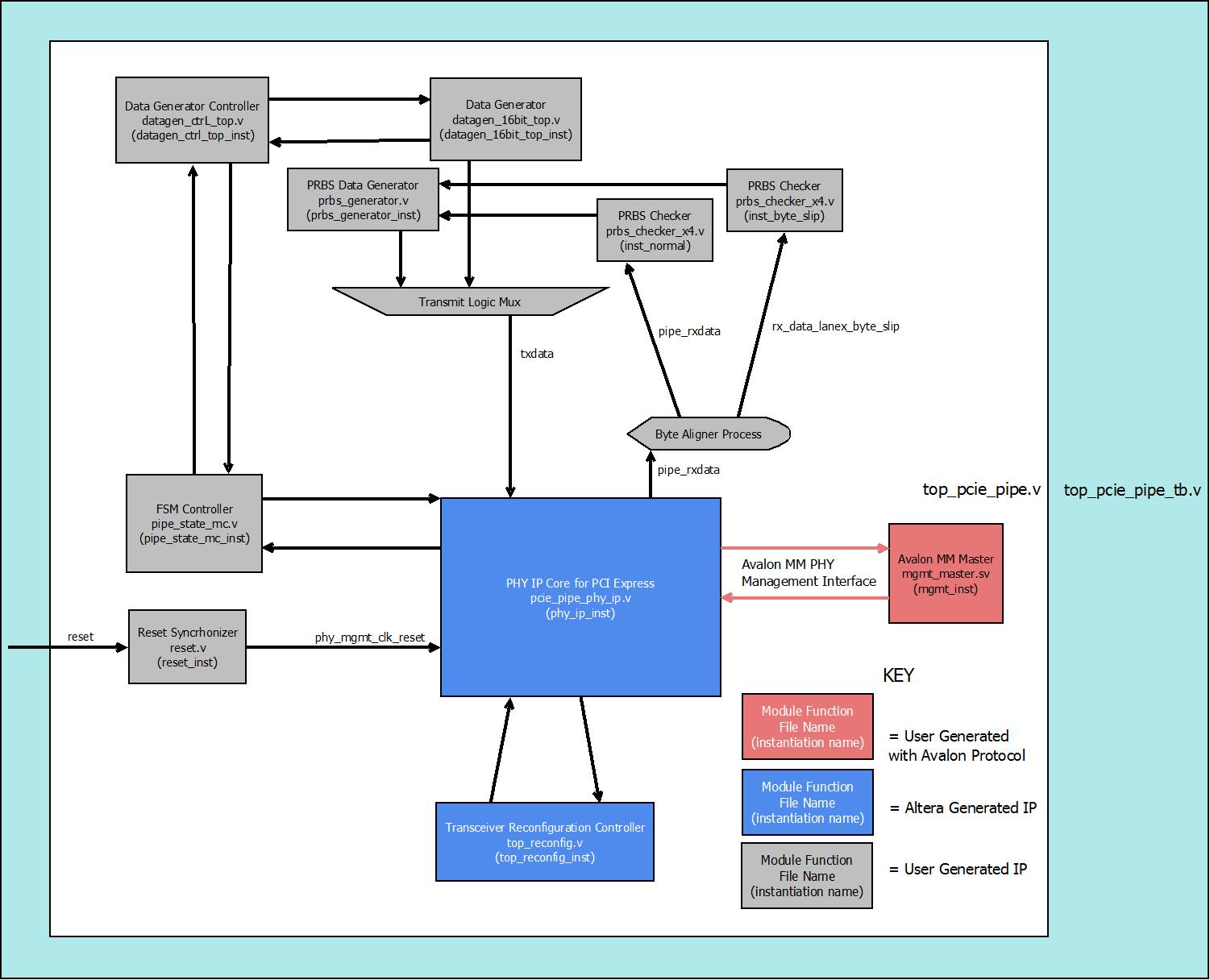
Please see figure 1-1 for a block diagram representing the components that make up the top level design file: top_pcie_pipe.v.
Figure 1-1: Top Level Block Diagram- PCI_Express_Top_Level_Block_Diagram.jpeg (Click here for image)
To view a larger version of the image, click on the image, then click on the image again once the new page loads, and then hold ctrl and scroll the mouse wheel to zoom in and out.
top_pcie_pipe (Top Level)
The Physical Layer imports 4 clocks: an input reference clock of 100 MHz, a fixed clock at 125 MHz, a management clock meant for the Avalon MM Interface of 150 MHz, and a reference clock for the frequency
checker. The input signal singal rate_switch_g1_to_g2_phase switches the PCIe configuration from Gen 1 to Gen 2.
pcie_pipe_phy_ip
Megawizard generated PCIe PHY IP. Please see the V-Series Transceiver PHY IP Core User Guidefor more information.
pipe_state_mc
Simple state machine that toggles the PIPE controls according to which state it is currently in.
| Current State | Next State | Condition To Move To Next State | Comments |
| Reset Phase | INIT_PHASE_G1 | Reset de-asserted | Gen 1, P1, Electrical Idle |
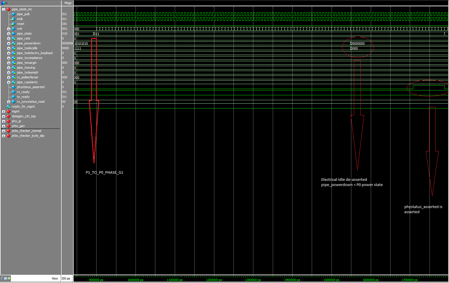
| INIT_PHASE_G1 | P1_TO_P0_PHASE_G1 | pipe_phystatus_reg = 0 | Gen 1, P1, Electrical Idle |
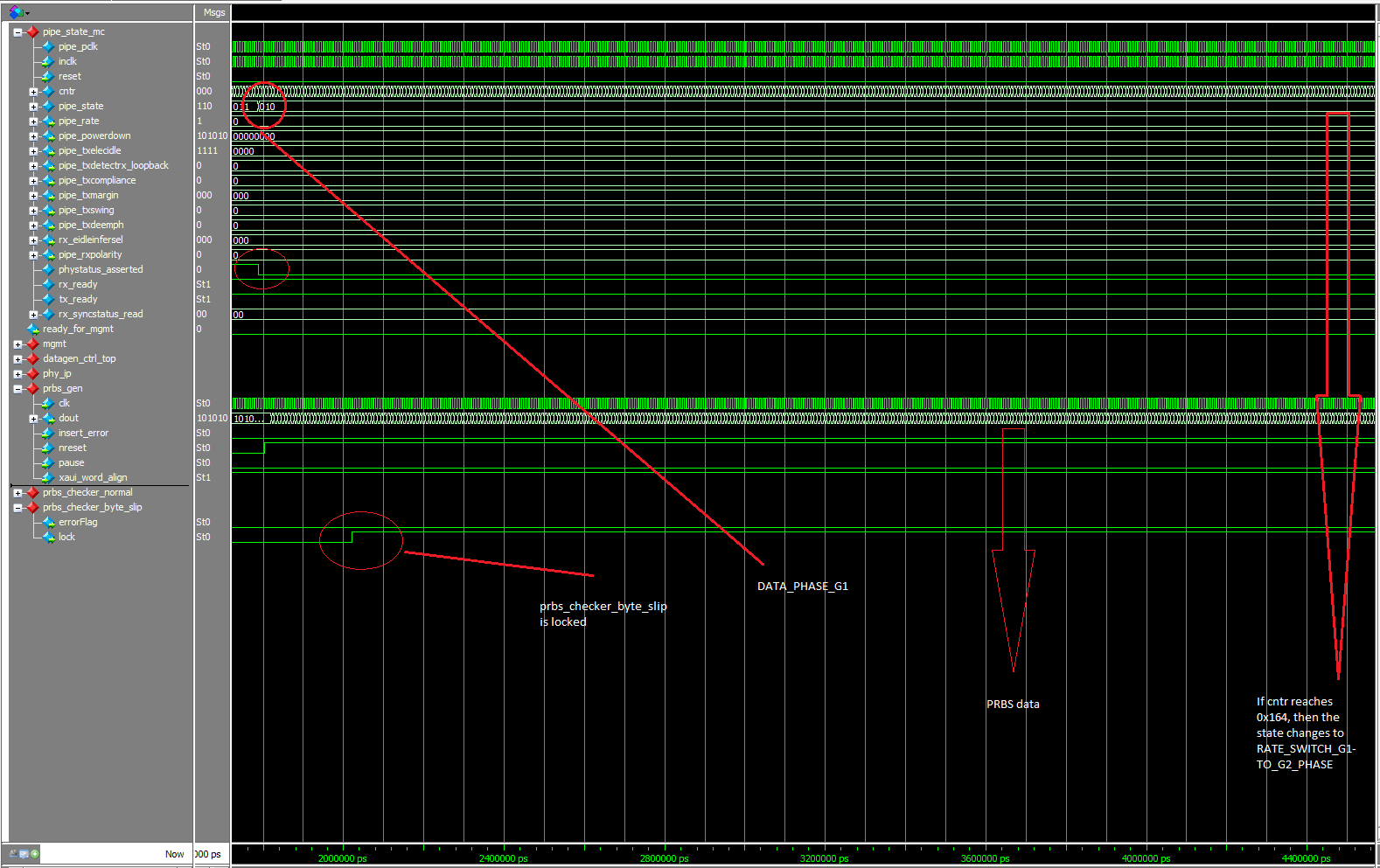
| P1_TO_P0_PHASE_G1 | DATA_PHASE_G1 | cntr >= 0x051 && cntr <= 0x164 & rx_syncstatus_reg = 0xFF (receiver is synced) | |
| DATA_PHASE_G1 | RATE_SWITCH_G1_TO_G2_PHASE | cntr == 0x164 (wait 0x164 clock cycles) | Gen 1, P0, Electricle Idle de-asserted |
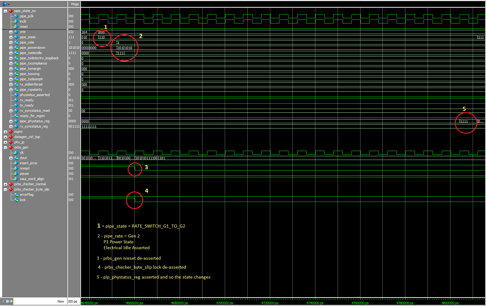
| RATE_SWITCH_G1_TO_G2_PHASE | P1_TO_P0_PHASE_G2 | pipe_phystatus_reg == 4'b1111 (rate switch from Gen 1 to Gen 2 succesful) | Gen 2, P1, Electricle Idle asserted |
| P1_TO_P0_PHASE_G2 | DATA_PHASE_G2 | cntr >= 0x051 && cntr <= 0x164 & rx_syncstatus_reg = 0xFF | |
| DATA_PHASE_G2 | Gen 2, P0, Electricle Idle de-asserted, ready_for_mgmt = 1 |
- Reset Phase = if the state machine's reset signal is asserted, the PHY IP is reset, and when the reset signal is de-asserted, the state machine moves to the INIT phase.
- INIT_PHASE_G1 = In this state, P1 power state is chosen, Gen 1 is chosen, and the PHY IP is put into electrical idle. Once the pipe_status_reg signal is de-asserted, the state moves to the transitional state between the INIT and DATA states.
- P1_TO_P0_PHASE_G1 = In this state, the state machine remains in the P1 power state for a few clock cycles (a counter counts to 0x050) and then moves to the P0 power state. When receive channel is synchronized the state machine moves to the data phase.
- DATA_PHASE_G1 = After the counter reaches 0x164 in this state, the state machine enters the tranisitional state between Gen 1 and Gen 2.
- RATE_SWITCH_G1_TO_G2_PHASE = In this state, the PHY IP enters the P1 power state, and switches to Gen 2.
- P1_TO_P0_PHASE_G2 = In this state, the the state machine waits until a counter reaches 0x050, and then transitions the PHY IP to the P0 power state and out of electrical idle. If the receive channel is syncrhonized, the state machine moves tot the data phase.
- DATA_PHASE_G2 = After a counter reaches 0x164, control is given to the Avalon MM interface, and the state machine remains in the DATA_PHASE_G2 state.
datagen_ctrl_top
This module gets the state transitions frompipe_state_mc and generates PIPE control signals and all the required controls for the data generator module.
datagen_16bit_top
Generates PIPE specific ordered sets corrseponding to the controls received from datagen_ctrl_top. This module instantiates datagen_16bit_x1 for 4 lanes. datagen_16bit_x1.v generates 16-bit data based on the controls received form datagen_ctrl_top.
prbs_generator
PRBS 23 pattern generator whos output is fed to the pipe_txdata during DATA_PHASE. All lanes get the same PRBS data.
prbs_checker_x4
PRBS 23 pattern checker that verifies the looped back PRBS data on pipe_rxdata. There are two checkers because of the uncertainty in the byte order of pipe_rxdata. Depending on the sampling time of the Byte SERDES in the Rx PCS, pipe_rxdata either has bytes ordered correctly or incorrectly. We need to check for these two cases. Therefore, byte ordering is done earlier in this module to correct for possible misordering.
mgmt_master
This module writes to/reads from the memory mapped registes inside of the Transceiver PHY IP through the Avalon PHY Management Interface (see the Avalon Specification for details). The Avalon-MM PHY management interface provides access to PIPE PCS and PMA features that are not part of the standard PIPE interface. This module is customized specifically for the PIPE. See the "Interfaces - Registers" section of chapter 6 of the V-Series Transceiver PHY IP Core User Guide.
Transmit Logic Multiplexor
Assigns parallel txdata of PIPE PHY IP - either data from the data generator or PRBS data from the prbs generator - to the txdata lanes of the PHY IP.
Miscellaneous
There is a module that syncrhonizes the brd_reset to the phy_mgmt_clk.
There is a process that synchronizes tx_ready and rx_ready to the pipe_clk.
There is a process that handles byte ordering of the rxdata.
Compilation in Quartus
1) Download and unzip the zip files linked above into a folder to be used as the download directory.
2) Open the project file (.qpf) by going to File > Open Project and navigating to <download_directory>\SV_PIPE\source. Open top_pcie_pipe.qpf.
3) Use the Megawizard Plug-in Manager to generate Altera Generated IP (labeled in figure 1-1)
Before compiling you must regenerate the Altera generated IP using the Megawizard. You will perform this step twice - once for the pcie_pipe_phy_ip.v and once for the top_reconfig.v. Open MegaWizard Plug-In Manager and choose edit a variation.
- Select the IP you want to edit and generate (The .v file will be located in your project directory).
- If your license for ModelSim can not support multiple HDL languages then chose verilog as output file type (The default settings will work for this example).
- Select the options for the IP you want to generate (The default settings will work for this example), and click Finish.
After completing the previous steps, you can compile the entire design by going to Processing > Start > Start Analysis and Synthesis.
4) During compilation you can expect following critical warnings
- Critical Warning (169085): No exact pin location assignment(s) for 28 pins of 28 total pins.
- Critical Warning: Timing requirements not met.
Compilation in ModelSim
You will need to create a .tcl script called phy_sim_top.tcl (there already exists a fully working phy_sim_top.tcl in the zip that contains the project files, however you will need to modify it if you add your own design files) that contains compilation commands for:
- Stratix V Library files
- PHY pcie_pipe_phy_ip Instance files
- Reconfig Controller instance files
- User created design files
- The Top Level Testbench file
- Commands to invoke the simulator
- make sure that the QUARTUS_ROOTDIR variable is set correctly in phy_sim_top.tcl. Note: the set QUARTUS_ROOTDIR $env(QUARTUS_ROOTIDIR) line sets the variable to the local systems version of quartus. To be safe, use set QUARTUS_ROOTDIR <your_quartus_root_directory>.
- It is important that the files in the .tcl be ordered as they are ordered in the plain_files.txt included in the zip file. The directory of the plain_files.txt is (<project_directory>\pcie_pipe_phy_ip_sim\altera_xcvr_pipe) for the pipe_phy_ip, and (<project_directory>\top_reconfig_sim\alt_xcvr_reconfig) for the reconfig_controller.
- It is recommended that you place all Altera generated IP into its own library.
Use the vlib <directory_name> command to create a design library. Use the following Tcl code as a reference:
vlib msim_pcie_pipe_phy_ip => creates a design library called msim_pcie_pipe_phy_ip in the current working directory.
Note that for ModelSim compilation, a vlog of the files is required before the vsim command. Use the vlog command to compile Verilog source code into a specified working library (or to the work library by default).
For example: vlog -work msim_pcie_pipe_phy_ip test.v => compiles the test.v file into the msim_pcie_pipe_phy_ip directory.
The -work <library_name> Specifies a logical name or pathname of a library that is to be mapped to the logical library work. By default, the compiled design units are added to the work library. If a pathname is specified, the specified pathname overrides the pathname specified for work in the project file.
If compiling a System Verilog file (.sv), you must place the "-sv" command after the "vlog" command and before the name of the file to be compiled.
After writing commands to create necessary libraries and compile design units, use the vsim command to invoke the modelsim simulator. Use the "-coption to run the simulation in command line mode. The -novopt option resolves certain compatibility issues. -t <number> sets the time scale to <number>.The -L <library_name>lets the simulator know where to look for design files when simulating.
Use this example script as a reference, and see this guide for a reference to using tcl commands in ModelSim.
Simulation Guidelines
The attached zip file has all the required design and simulation files. To start the simulation, launch Modelsim and source phy_sim_top.tcl
Annotated timing diagrams of the proper operation of the 6 states of pipe_state_mc are provided for your reference.
Figure 2-1 : INIT_PHASE_G1- P1_TO_P0_PHASE_G1_annotated.png (Click here for image)
Figure 2-2 : DATA_PHASE_G1- DATA_PHASE_G1_annotated.png (Click here for image)
Figure 2-3: RATE_SWITCH_G1_TO_G2_PHASE- RATE_SWITCH_G1_TO_G2_annotated.png (Click here for image)
Figure 2-4: P1_TO_P0_PHASE_G2- P1_TO_P0_PHASE_G2_annotated.png (Click here for image)
Figure 2-5: DATA_PHASE_G2-DATA_PHASE_G2_annotated.png (Click here for image)
Update History
- Initial Release - May 05 2011
See Also
Key Words
Stratix V, PCIE PIPE PHY IP, Tranceiver Reconfiguration Controller, Physical layer, PCI Express, Express, Stratix Five, GT, GS, GX, Design, Example, guide, walkthrough,
PCIe, PCI E, PCI Express, Stratix V, SV, S, V, Walkthrough, guide, help, Stratix V GX, Stratix V GT, SV, SVGX, SVGT, S5GX, S5GT, S5, Stratix 5, Stratix 5 GX, StratixV, StratixV GX, Stratix5, Stratix5 GX, Altera, generated, generation, Instantiation, creation, design, files,
© 2010 Altera Corporation. The material in this wiki page or document is provided AS-IS and is not
supported by Altera Corporation. Use the material in this document at your own risk; it might be, for example, objectionable,
misleading or inaccurate.
Community support is provided Monday to Friday. Other contact methods are available here.
Intel does not verify all solutions, including but not limited to any file transfers that may appear in this community. Accordingly, Intel disclaims all express and implied warranties, including without limitation, the implied warranties of merchantability, fitness for a particular purpose, and non-infringement, as well as any warranty arising from course of performance, course of dealing, or usage in trade.
For more complete information about compiler optimizations, see our Optimization Notice.