IBIS AMI
Success! Subscription added.
Success! Subscription removed.
Sorry, you must verify to complete this action. Please click the verification link in your email. You may re-send via your profile.
IBIS AMI
- Subscribe to RSS Feed
- Mark as New
- Mark as Read
- Bookmark
- Subscribe
- Printer Friendly Page
- Report Inappropriate Content
IBIS AMI
This document describes the advantage of IBIS-Algorithmic Modeling Interface (AMI) in high-speed transceiver link simulation. It first introduces basic knowledge about IBIS-AMI and then compares IBIS-AMI model with transitional Hspice model. In addition, a design example is walked through to provide guidance on high speed serial link design with Altera FPGAs.
Introduction
Multi-gigabit serial link (SerDes) channels are rapidly becoming the primary mechanism used to transfer high-speed data. Performing the link simulation is critical to determine if a link meets the design requirements based on the selected transmitter, receiver and backplane in between. SerDes protocols usually require verifying the system to low bit-error-rate (BER) to ensure the system performance. Traditional signal integrity simulation with Hspice-based analysis can’t simulate millions of bits due to slow simulation speeds. Hspice simulations also have difficulty including crosstalk and jitter impairments.
The new modeling methodology with IBIS-AMI addressed most of the link simulation requirements, such as simulating millions of bits in minutes, crosstalk/jitter analysis and data pattern dependencies. It also adds a mixed-signal model capability to IBIS standard by introducing algorithmic modeling components, which allows IBIS-AMI to model complex blocks, such as equalization, DFE and CDR.
This white paper discusses how to perform link simulations with IBIS-AMI models, provide insight into stressing the link with various data patterns and incorporating crosstalk and jitter into the IBIS-AMI simulations for system link performance analysis.
This white paper is organized as follows. First, an introduction of the IBIS-AMI standard development background, IBIS-AMI model kit file structure, and its simulation flow are provided. Second, the advantages of IBIS-AMI simulations over Hspice simulations with regard to BER analysis, data pattern analysis, crosstalk and jitter analysis are described. Lastly, an explanation of how IBIS-AMI helps with high speed SerDes link design with a customer example is shown.
IBIS-AMI Standard Development Background
Input/Output Buffer Information Specification (IBIS) has been an essential electrical simulation model for many years. It provides an accurate and easy-to-use alternative to SPICE based transistor model. As the circuit is modeled behaviorally in IBIS, simulation speed is fast. As serial interface data rates increase, signal processing blocks are used to compensate the channel loss. These blocks include Feed-Forward Equalization (FFE), Linear Equalization, Decision Feedback Equalization (DFE), and Clock Data Recovery (CDR). Conventional behavior IBIS models do not capability to model these mix-signal signal processing blocks.
SerDes designers have used various mixed-signal modeling tools such as Matlab, Verilog-AMS and VHDL-AMS to co-simulate the digital and analog parts of transceivers. IC vendors are reluctant to release the algorithmic code used to implement the digital pieces since it contains valuable IP. A system engineer interested in the overall channel behavior would have to model the transceivers behaviorally using generic macro models or create custom algorithmic functions in a tool such as MATLAB. Without specific knowledge of a particular transceiver design, this task is difficult. Several SerDes vendors, such as IBM, with its HSSCDR MATLAB-based simulator, provide models embedded and distributed with its proprietary simulator tool. Unfortunately, this tool is not interoperable between IC or EDA tool vendors.
In 2005, the IBIS committee introduced the Algorithmic Interface Model (IBIS-AMI) standard to address these challenges [1]. IBIS-AMI is an extension to the IBIS standard. It allows high speed transmitter and receiver models to be supplied as executables. Due to the flexibility of executables, complex signal processing blocks can be modeled algorithmically. AMI models also enable standardized, interoperable simulation of SerDes with high simulation speed, performance and accuracy. Crosstalk and jitter analysis may be added while maintaining fast simulation speeds.
In addition to strong modeling and simulation capabilities, IBIS-AMI has a number of other benefits, which allowed it to become an industry standard.
- Interoperability – Models from different semiconductor vendors run together in the same simulation
- Transportability – The same model runs in different simulators
- Accuracy – IBIS-AMI based simulations provide results comparable to those obtained with proprietary semiconductor vendor tools
- IP Protection – Semiconductor vendors are able to provide accurate models of their devices without divulging internal architectural details
IBIS-AMI File Structure
An IBIS-AMI model kit has three model files, IBIS file (.IBS), AMI parameter file (.AMI), and algorithmic executable file (typically .DLL in window OS and *.OS in Linux OS). The ASCII-text IBIS file contains keyword [Algorithmic Model] to point to the algorithmic executable file and AMI parameter file, and to declare the operation system. The IBIS file also models un-equalized transceiver electrical characteristics. For Altera IBIS-AMI models, the IBIS file contains the following elements:
- Transmitter without equalization: output voltage swing, impedance, slew rate, output parasitic
- Receiver without equalization: input termination impedance and parasitics
The algorithm parameter file (.AMI) is a simple ASCII-text file. The parameter file contains two main sections. The first section lists [Reserved_Parameters] that define the model processing flows, such as the Init_Returns_Impulse and GetWave_Exists declarations. This section may also be edited to add jitter parameters such as Tx_Jitter or Rx_Clock_PDF. The second section is listed under the keyword [Model_Specific] and is used to pass simulation parameters to the executable for configuring the behavior of the model, such as equalization and CDR configuration.
The algorithmic portion of IBIS-AMI model is a behavioral model, which contains the signal processing functions and is supplied as executables. For the Altera IBIS-AMI models, the algorithmic portion models the following transceiver elements:
- Transmitter: Pre-emphasis
- Receiver: CTLE (continuous time linear equalizer), DFE (Decision Feedback Equalization), CDR (clock data recovery), ADCE (Adaptive Dispersion Compensation Engine)
All IBIS-AMI model files are assumed to be located in the same directory, so that the EDA tool can resolve the location pointers.
IBIS-AMI Simulation Flow
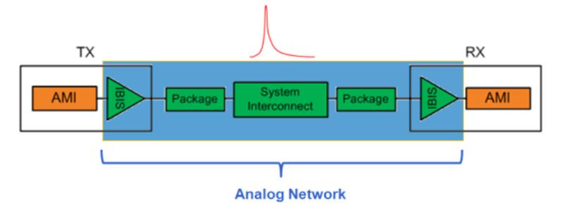
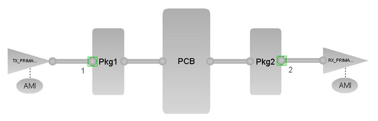
Fig 1 gives a typical example of an IBIS-AMI model simulation in an EDA platform. IBIS-AMI models are simulator independent, so any IBIS-AMI model may be run on any EDA simulator that supports IBIS-AMI. Below, Sigrity Channel Designer is chosen to illustrate the simulation process and outcomes. The simulation setup usually consists of three major elements: the transmitter IBIS-AMI model, the transmission path, and the receiver IBIS-AMI model. The transmission path can consist of interconnects, like the printed circuit board (PCB), packages, connectors, etc.
a/a1/IBIS-AMI1.JPG ( IBIS-AMI1.JPG - click here to view image )
Figure 1 Typical SerDes link IBIS-AMI simulation setup
Simulator processes the simulation in two stages: network characterization, and channel analysis. Network characterization uses spice-based simulator to simulate the impulse response of an analog network that includes: the analog portion of transmitter, the transmission path, and the analog portion of receiver. Fig. 2 illustrates the network characterization process.
uploads/a/a5/IBIS-AMI2.JPG ( IBIS-AMI2.JPG - click here to view image )
Figure 2 Network Characterization
After network characterization, channel analysis takes the impulse response created by network characterization and uses algorithmic models of equalization and clock recovery to post-process the impulse response to simulate the entire link behavior and plot eye diagram, bathtub curve, and eye contour, etc. Channel analysis is very different from traditional Hspice simulations. It uses signal processing techniques, such as convolution to perform the simulation. Two types of channel analysis exist, which has their own pros and cons.
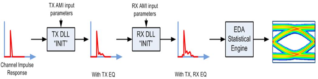
Statistical analysis [2] produces an eye diagram showing the probabilities of signal distribution at the receiver without using a specific data pattern. Statistical analysis has the advantage of fast simulation speeds, simulating approximately 1012 bits per minute. However, statistical analysis can only implement linear time invariant (LTI) algorithms, such as CTLE, but not non-LTI blocks, such as DFE. To overcome this drawback, Altera IBIS-AMI models implement an approximated DFE model, which is modeled as an LTI block, in statistical analysis. This improves simulation accuracy, comparing to no DFE model. In addition, as statistical analysis does not have bit stream information, it is not able to provide recovered clock and model CDR.
Statistical analysis flow is shown in Fig 3. The channel impulse response from network characterization is first passed to the transmitter’s AMI_Init() function. The transmitter’s AMI_Init() function applies a feed-forward equalization (FFE) signal processing algorithm (transmitter pre-emphasis) to the channel impulse response and outputs the equalized transmitter’s impulse response. This impulse response is further passed to the receiver’s AMI_Init() function, where linear equalization (CTLE) and approximated LTI DFE signal processing algorithms are applied. Finally, the transmitter and receiver equalized impulse response is produced. The EDA tool processes the equalized impulse response to compute the eye probabilities and BER statistically.
9/99/IBIS-AMI3.JPG ( IBIS-AMI3.JPG - click here to view image )
Figure 3 Statistical Analysis Flow
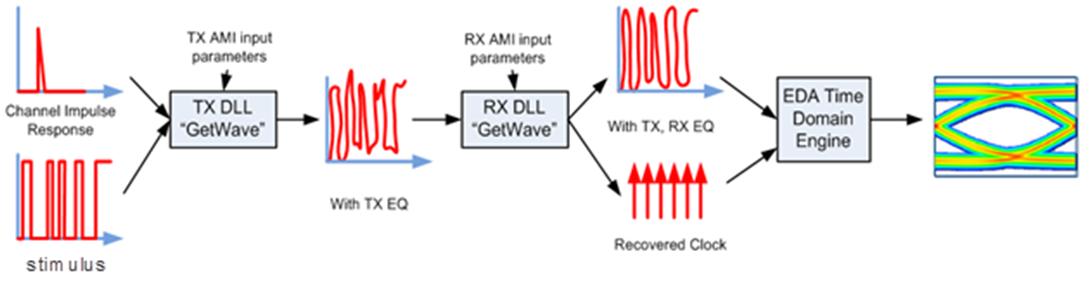
Time-Domain analysis behaves much like traditional SPICE-based analysis, which generates bit by bit time domain waveform. In time-domain analysis, the input stimulus is convolved with the channel impulse response and a waveform representing the circuit’s behavior is generated. Time-domain analysis speeds are relatively slow. It typically runs at millions bits per minute. This form of analysis is good for modeling non-LTI blocks, such as the adaptive behavior of DFE control loops, and can model clock recovery circuitry.
There are several time-domain analysis flow options. Here we only discuss the flow used in Altera IBIS-AMI models. Fig 4 illustrates the time-domain analysis flow of Altera models. The EDA simulation tool generates stimulus depending on bit rate and data pattern, and convolves the stimulus with the channel impulse response. The transmitter AMI_Getwave() function applies the FFE algorithm to the convolved waveform to produce the transmitter equalized time-domain waveform. Subsequently, the receiver AMI_Getwave() function takes this waveform and applies linear equalization and the DFE signal processing algorithms to generate the time-domain waveform at the receiver output. Meanwhile, receiver AMI_Getwave() function also recovers the clock from the input data stream. Finally, the EDA tool computes the eye probabilities and BER from the equalized waveform and recovered clock.
8/81/IBIS-AMI4.JPG ( IBIS-AMI4.JPG - click here to view image )
Figure 4 Time-domain Analysis Flow
Fig 5 shows examples of channel analysis graphical outputs, such as the time domain waveform, eye diagram, bathtub curve, and eye contour at the Rx output. Due to fast channel analysis capability, IBIS-AMI models can simulate BERs below 10-12. This satisfies all the high speed SerDes protocol simulation requirements.
6/62/IBIS-AMI5.JPG ( IBIS-AMI5.JPG - click here to view image )
Figure 5 IBIS-AMI Simulation Outputs
IBIS-AMI Advantages
Data Pattern Simulation
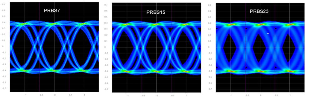
Link performance highly depends on stimulus’s data pattern. For the same link, a PRBS7 data pattern may easily pass an eye mask requirement. But a PRBS31 data pattern may fail the eye mask even with maximum equalization gain. Long 0s and long 1s that are present in PRBS31 patterns generate more ISI jitter than PRBS7 patterns and close the eye at the Rx input further.
Traditional Hspice models are transistor level models that include all circuit detail. The simulation accuracy is high. As transistor sizes decrease, transistor models become more complicated, and simulation times increase greatly. Because of increased simulation times, system designers can only afford to simulate PRBS7 patterns and are not able to fully explore the design space by configuring different equalization settings.
Fast simulation speed of IBIS-AMI models allows long bit sequence simulations. As mentioned in section 4, statistical analysis can simulate ~1012 bits per minute and time domain analysis can simulate ~106 bits per minute. Based on the bits simulated per minute, statistical analysis can simulate PRBS31 data pattern, but time domain analysis is typically limited to PRBS23 or below. Most EDA tools, however, provide an extrapolation option to extend the time domain analysis results to a lower BER.
Fig 6 illustrates how the eye diagram changes with data pattern in the same serial link. IBIS-AMI simulation is used to generate these results. In this simulation, only ISI jitter is included. As we can see from the figure, the PRBS7 pattern gives a quite clean eye. As the bit sequence becomes longer, the eye width and eye height become smaller. PRBS23 pattern has a great amount of ISI jitter. If system designer use traditional Hspice model and simulate only PRBS7 pattern, the outcomes could be misleading and optimistic. By using IBIS-AMI simulation, designers can avoid obtain the optimistic result and verify the system performance with the real system data pattern.
f/f3/IBIS-AMI6.JPG ( IBIS-AMI6.JPG - click here to view image )
Figure 6 Eye Diagram with Various Data Pattern
Jitter Simulation
As the transceiver data rate increases, the jitter from the transmitter and receiver play an important role in the link performance. In 10Gbps serial links, the intrinsic transceiver jitter can contribute up to 0.3 UI. Intrinsic jitter turns out to be so significant that it cannot be excluded from link simulations.
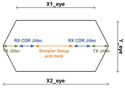
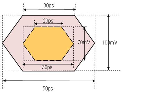
Traditional Hspice models only model a small portion of deterministic jitter (Dj) from Tx/Rx equalization. It doesn’t include Dj from clock trees and CDR, Tx/ Rx intrinsic random jitter (Rj) etc. As a result, Hspice model simulation results only include ISI jitter from the transmission path, with little or no Tx/Rx intrinsic deterministic jitter. To calculate BER with Hspice simulation results, Altera provides a jitter guard band eye mask. Fig 7 shows the Altera Hspice model eye mask at the output of Rx CTLE block. This eye mask consists of not only sampler setup and holds time, but also budget for Tx intrinsic jitter and Rx CDR intrinsic jitter. While using jitter guard banded eye mask, no additional Altera device intrinsic jitters need to be included in simulation.
c/cb/IBIS-AMI7.JPG ( IBIS-AMI7.JPG - click here to view image )
Figure 7 Altera Eye Mask Composition
While jitter guard banded eye mask is easy to use, it has some disadvantages. FPGAs are programmable devices, which have different intrinsic jitter with different configurations, such as PLL types, PVT conditions etc. The fixed jitter guard banded eye mask cannot reflect the intrinsic jitter variance with different transceiver configurations. To cover all system applications, the jitter guard bands are obtained based on the worst case scenario. Fig 8 compares the Stratix V device eye masks with and without jitter guard band at 10.3Gbps data rate. As shown in figure, the jitter guard banded eye mask is much larger, compared to the sampler eye mask. For most system applications, this worst case scenario eye mask will underestimate the system performance.
2/21/IBIS-AMI8.JPG ( IBIS-AMI8.JPG - click here to view image )
Figure 8 Stratix V eye mask comparison
(solid line: eye mask with jitter guard band; dotted line: sampler eye mask, no jitter guard band)
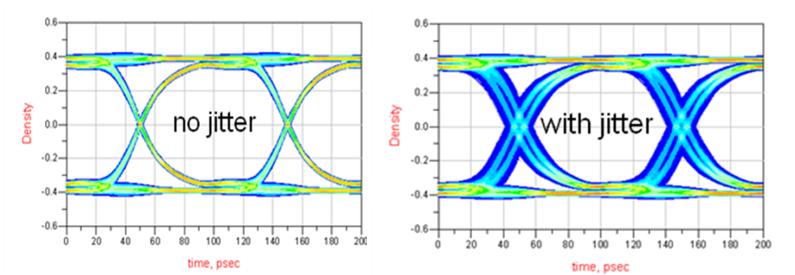
IBIS-AMI allows the inclusion of Tx/Rx jitter in simulation simply by specifying the jitter amount through model parameters. Altera has fully characterized the Tx/Rx jitter contribution from hardware under different transceiver configurations, such as data pattern, PVT condition, PLL type and bandwidth. Designers can use the Altera in-house tool, Jitter and BER estimator (JBE), to look up the jitter amount of their system and include jitter in their IBIS-AMI simulation. With the capability of jitter simulation, IBIS-AMI models can use the sampler’s eye mask, instead of the jitter guard banded eye mask, to evaluate the system performance. This avoids overestimation of the jitter noise and gives more margins on timing requirements. Fig 9 gives an example of comparison of IBIS-AMI simulation with and without jitter. In this example, only the Tx buffer is simulated where 6ps Tx Dj and 1.35ps Tx Rj(RMS) are added in the jitter analysis. One million bits are simulated in both cases.
f/fe/IBIS-AMI9.JPG ( IBIS-AMI9.JPG - click here to view image )
Figure 9 IBIS-AMI Simulation Results with/without Jitter
Crosstalk Simulation
Crosstalk is the unwanted coupling of signals from IC packages, parallel traces, connectors, etc. In high speed system, crosstalk becomes a more prominent concern than ever before, due to higher IC I/O density caused by smaller transistor geometries, increasing PCB board routing density, and high density connectors. In high speed simulations, there are increasing demands to include crosstalk analysis in the design process.
Hspice simulations are very time consuming as it needs to process the transistor level circuit. To analyze crosstalk, Hspice simulations have to simulate multiple sets of transceiver channels. It is not feasible to simulate multiple transceiver channels within a reasonable time. In addition, when multiple buffer models are included in the Hspice simulation, this is likely to lead to simulation convergence issues.
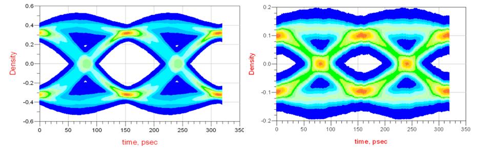
In EDA platforms that support multi-port coupling, IBIS-AMI simulation extracts the impulse response from aggressor drivers to the victim receiver. It superposes the crosstalk impulse response on the primary channel’s impulse response to produce the crosstalk waveform. Crosstalk simulation time is roughly N times of one transceiver channel simulation time, where N is the aggressor transceiver channel number. Fig 10 compares the simulation results with and without crosstalk. The crosstalk simulation has five adjacent transceiver channels as aggressors. As we can see from the comparison, by only adding crosstalk effect from other transceiver channels, the system performance changes and eye quality degrades significantly. IBIS-AMI allows system designers to capture crosstalk effects at the pre-layout stage to shorten design cycles.
e/e0/IBIS-AMI10.JPG ( IBIS-AMI10.JPG - click here to view image )
Figure 10 IBIS-AMI simulation results with/without crosstalk
(Left: no crosstalk; Right: with crosstalk)
High Speed Serial Link Design Example
Altera provides a complete transceiver solution kit, which contains transceiver models, in-house tools, and a signal integrity development board to aid system designers in PCB design and system verification. This kit greatly reduces system design time and shortens time-to-market. Fig11 shows the Altera recommended SerDes link simulation flow. A customer system design example is provided to explain how to design a high speed serial link with IBIS-AMI models and other Altera tools.
e/e9/IBIS-AMI11.JPG ( IBIS-AMI11.JPG - click here to view image )
Figure 11 Altera Serial Link Design Flow
At the beginning of the design, system designers need to select the Altera FPGA device that best meet the system’s requirements such as the number of I/O pins, clock pins, and number of transceivers required, etc. In this example, a Stratix V GX device is selected.
Once the design has progressed far enough so that the channels are understood, s-parameters need to be obtained. This may be accomplished either through pre-layout or post-layout simulation in EDA 2.5D or 3D simulation tool. If crosstalk analysis is desired, multiple ports S parameter should be generated. Fig 12 shows the primary channel insertion loss of a 12-port channel S parameter that used in this example.
e/e7/IBIS-AMI12.JPG ( IBIS-AMI12.JPG - click here to view image )
Figure 12 Insertion Loss of a 12-port S Parameter
Altera’s transceiver devices contain Tx pre-emphasis and Rx equalization blocks such as FFE, DFE and CTLE to compensate channel attenuation effects. It is necessary to select optimal pre-emphasis and equalization levels, because both under and over compensation will increase the jitter in the link. Thousands of Tx pre-emphasis and Rx equalization setting combinations exist in Altera transceivers. Manually searching optimal settings may take weeks or months. The in-house behavior transceiver model tools, pre-emphasis and equalization link estimator (PELE), can be used to find the optimal settings based on the channel S parameter in minutes.
However, PELE has several limitations. First, PELE only has PRBS7 and PRBS10 data patterns. Second, PELE assumes a 100 Ohm system and does not consider reflections from impedance mismatch. Third, jitter cannot be included during the optimization. Therefore, without considering jitter, reflection and data patterns, PELE provides optimistic eye height and eye width estimations. The optimal pre-emphasis and equalization settings from PELE may be deviated from true optimal settings. It provides initial estimated pre-emphasis and equalization settings. IBIS-AMI must be used to fine-tune the settings and calculate a more accurate eye diagram and BER plot. By importing the channel S parameter in Fig 12 to PELE, PELE calculates the estimated settings, which are listed in Table 1.
If jitter simulation is desired, Altera has another in-house tool, Jitter and BER estimator (JBE), which reports the Dj and Rj of Tx and Rx based on hardware characterization. The jitter data is collected with different transceiver configurations, such as PVT condition, PLL type and PLL bandwidth. In this example, based on the transceiver configuration, JBE reports 0.986ps Tx Rj(RMS), 4ps Tx Dj, 2.13ps Rx Rj(RMS) and 2.52ps Rx Dj.
IBIS-AMI models are used to fine-tune and validate the settings. The user can select user defined patterns to perform link simulations and run crosstalk and jitter analysis. Statistical analysis is used first for initial design space exploration, since statistical analysis has fast simulation speed. Time-domain analysis is used after that to get more accurate simulation results. These time domain analysis results can be leveraged to determine the system BER. Fig 13 illustrates the IBIS-AMI simulation setup.
5/50/IBIS-AMI13.JPG ( IBIS-AMI13.JPG - click here to view image )
Figure 13 IBIS-AMI Simulation Setup
In this example, after fine-tuning with the IBIS-AMI simulator, it was determined that PELE already gives the best EQ settings. Using the EQ settings listed in Table 1, the IBIS-AMI simulation outputs the eye opening and BER plot as shown in Table 1. As is shown from the table, the IBIS-AMI eye opening is much smaller than the PELE eye opening. This is mainly due to crosstalk and jitter analysis in the IBIS-AMI simulation. The IBIS-AMI simulation results show that this link meets a 10-15 BER.
Table 1 PELE and IBIS-AMI results of optimal EQ settings and eye opening
| PELE | IBIS-AMI | ||
| TX | Vod | 2 | 2 |
| pre-tap | 0 | 0 | |
| post-tap1 | 0 | 0 | |
| post-tap2 | 0 | 0 | |
| RX CTLE | AC Gain | 14 | 14 |
| DC Gain | 4 | 4 | |
| RX DFE | tap1 | 0 | 0 |
| tap2 | -1 | -1 | |
| tap3 | 1 | 1 | |
| tap4 | 0 | 0 | |
| tap5 | -1 | -1 | |
| Eye Width | 0.77UI | 0.65UI | |
| Eye Height | 630mV | 579mV | |
Based on the IBIS-AMI results, make sure the eye-opening requirements for the selected protocol standard are met, both at the near and far end, if required. If any requirement is not met, the designer must redesign the communication channel and re-do the procedures described above. Altera provides a signal integrity board evaluation kit to evaluate the device in early design stage for verify and debug in hardware, as an optional step. At last, based on the simulation results and hardware testing, the design of high speed serial link is finalized.
Conclusion
This white paper introduces the new industry model standard, IBIS-AMI. From an application point of view, this paper states the need of new model methodology in high speed link simulation. IBIS-AMI specification meets most of the high speed serial link simulation requirements. The algorithmic modeling capabilities can model complex transceiver blocks, like DFE and CDR, and run simulation at million bits per minute. IBIS-AMI also provides crosstalk and jitter analysis. With this simulation capability, designers are able to confidently design their systems and estimate their system performance and margin.
Community support is provided Monday to Friday. Other contact methods are available here.
Intel does not verify all solutions, including but not limited to any file transfers that may appear in this community. Accordingly, Intel disclaims all express and implied warranties, including without limitation, the implied warranties of merchantability, fitness for a particular purpose, and non-infringement, as well as any warranty arising from course of performance, course of dealing, or usage in trade.
For more complete information about compiler optimizations, see our Optimization Notice.