Implementing MSI-X for PCI Express in Altera FPGA Devices
Success! Subscription added.
Success! Subscription removed.
Sorry, you must verify to complete this action. Please click the verification link in your email. You may re-send via your profile.
- Intel Community
- Intel Community Knowledge Base
- Product Support Forums Knowledge Base
- FPGA Knowledge Base
- FPGA Wiki
- Implementing MSI-X for PCI Express in Altera FPGA Devices
Implementing MSI-X for PCI Express in Altera FPGA Devices
- Subscribe to RSS Feed
- Mark as New
- Mark as Read
- Bookmark
- Subscribe
- Printer Friendly Page
- Report Inappropriate Content
Implementing MSI-X for PCI Express in Altera FPGA Devices
Introduction
This article explains how to implement PCIe MSI-X interrupt in Altera FPGA devices. The article is separated into two parts. The first part explains what is MSI-X and how to use it in a PCIe system. The second part explains how to implement it in the FPGA.
MSI-X Background
Why Use MSI-X Interrupts
MSI-X allows a larger number of interrupts compare to MSI interrupts, it gives each one a separate target address and data word.
MSI-X defines a separate extension to basic MSI functionality. Compared to MSI, MSI-X supports a larger maximum number of vectors per function, the ability for the software to control each vector, and the ability for each vector to use an independent set of address and data values. All this is implemented through a table which resides in the device’s memory space.
MSI-X Introduction
MSI-X is an optional feature that provides a method of in-band signaling of an interrupt. This feature enables a device function to request service by writing a system-specified data value to a system-specified address. System software initializes the message address and message data during device configuration.
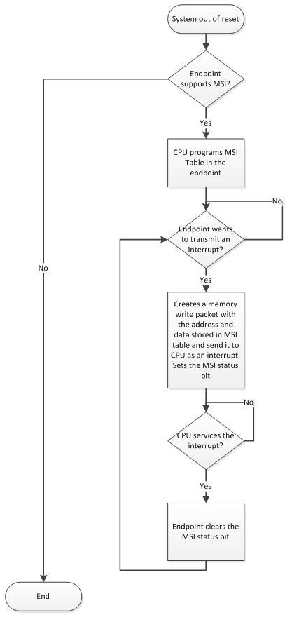
Figure 1 shows the flow diagram for MSI interrupt (MSI-X is similar to the flow diagram as below too).
a/ad/Msix_figure1.png ( Msix figure1.png - click here to view image )
Figure 1 - MSI Generation and Handling Flow
A function is permitted to implement both MSI and MSI-X, but only one is allowed to be enabled at a time. If the system software enables both at the same time, the result is undefined.
For the sake of software backward compatibility, MSI and MSI-X use separate and independent capability structures.
MSI-X Capability and Table Structures Programming
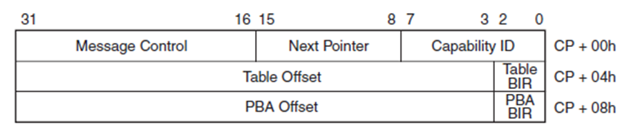
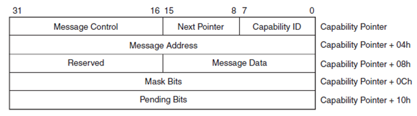
For comparison purpose, the MSI-X capability structure is illustrated in Figure 2 below and the MSI capability structure is shown in Figure 3 as a reference. Each function can only have one MSI-X capability structure.
9/99/Msix_figure2.png ( Msix figure2.png - click here to view image )
Figure 2 - MSI-X Capability Structure
9/98/Msix_figure3.png ( Msix figure3.png - click here to view image )
Figure 3 - MSI Capability Structure
Compared to the MSI capability structure, the MSI-X capability structure does not contain all controls and status information. The MSI-X capability structure instead points to a MSI-X Table structure and a MSI-X Pending Bit Array (PBA) structure, both of them reside in the device’s memory space. Each structure is mapped to the device’s memory space by a PCIe BAR which is located beginning at offset 10h in the Configuration Space.
The Table BIR (BAR Indicator Reigster) and PBA BIR in the MSI-X capability structure indicates which PCIe BAR the structure is mapped to. For example, if the value in BIR is 0, it means the structure is mapped through PCIe Bar0 at offset 10h in the Configuration Space. If the value in BIR is 1, it means the structure is mapped through PCIe Bar1 and so on. The BAR is permitted to be either 32-bit or 64-bit, but the BAR must be memory mapped, not mapped to IO space. The two structures can be mapped to the same BAR or two different BARs.
The Offset is QWORD-aligned and indicates where the structure begins relative to the base address associated with the BAR.
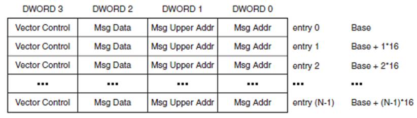
The MSI-X Table Structure contains multiple entries and eachentry represents one interrupt vector. Each entry has 4 QWORDs and consists of a32-bit lower Message Address, 32-bit upper Message Address, 32-bit data, and asingle Mask bit in the Vector Control field as shown in Figure 4 below. When the device wants to transmit a MSI-X interrupt message, it does
- Picks up an entry in the Table Structure, sendsout a PCIe memory write with the address and data in the table to the system host.
- Sets the associated bit in the PBA structure to represent which MSI-X is prepared to be sent and the bit is set before MSI-X interrupt is sent. The bit is set when the corresponding MSI-X vector is masked, it means there is MSI-X is pending, the message is not sent out because the vector is masked. When the vector is unmasked, the message is out and the PBA bit is cleared.
- After the MSI-X message is sent, the function which generates the MSI-X interrupt clears the bit.
f/f6/Msix_figure4.png ( Msix figure4.png - click here to view image )
Figure 4 - MSI-X Table Structure
The MSI-X PBA Structure is shown Figure 5 below. Each pending bit is associated with one entry in the MSI-X Table Structure.
3/3b/Msix_figure5.png ( Msix figure5.png - click here to view image )
Figure 5 - MSI-X PBA Structure
The number of interrupts a function can generate depend on the number of entries in the Table Structure. This is defined when configuring the PCIe HIP and this value is reflected in the Table Size portion of the Message Control register. This read only register is part of the MSI-X Capability Structure. The system software will read this field to determine the size of the table and then configure the MSI-X Table Structure. For example, if the software reads back the value of 3, it means the table has 4 entries, from entry 0 to entry 3
Enabling and Implementing MSI-X with Altera PCIe Hard IP (HIP)
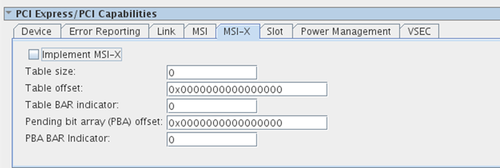
Altera PCIe HIP contains the MSI-X Capability Structure, but not the Table and PBA structures. When the user configures the HIP in Qsys, the parameters of the MSI-X Capability Structure need to be filled in, so Quartus II can generate the IP as requested. Select the MSI-X tab in PCI Express/PCI Capabilities section. Enable the Implement MSI-X option, fill in the parameters, such as the Table Size, Table Offset, Table BAR Indicator (Table BIR), Pending bit array (PBA) Offset, and PBA BAR Indicator (PBA BIR) as shown in Figure 6.
Altera PCIe Hard IP core supports up to 2048 MSI-X Table size. Legal range is 0–2047.
5/51/Msix_figure6.png ( Msix figure6.png - click her to view image )
Figure 6 - MSI-X Tab when Configuring PCIe HIP in Qsys
Table size states the size of the MSI-X Table. The offset tells the memory map offset of the structure in the PCIe BAR. The BAR indicator decides which PCIe BAR the structure is mapped to.
For the Table Structure and PBA Structure, both of them are implemented in user application logic. They can be implemented using on-chip memory or registers in the FPGA. The Figure 7 shows a block diagram where the two structures use two separated BARs and both of them have zero offset. The MSI-X Table structure uses BAR0 in the PCIe configuration space and the PBA Structure uses BAR1.
7/7f/Msix_figure7.png ( Msix figure7.png - click here to view image )
Figure 7 - Example Implementation of MSI-X Table and PBA through two BARs
Two MSI-X structures can be mapped to one BAR, but the two structures should have two different offsets and must not overlap. Figure 8 shows the block diagram of this implementation. In the example, both structures are mapped to BAR2 in the PCIe configuration space. The MSI-X PBA structure has offset 0 and MSI-X Table structure has offset 1000h.
d/df/Msix_figure8.png ( Msix figure8.png - click here to view image )
Figure 8 - Example Implementation of MSI-X Table and PBA through one BAR
For Avalon-ST designs, user logic can determine whether the BAR is hit by monitoring rx_st_bardec1 or rx_st_bardec1 and rx_st_bardec2 depending on the PCIe HIP configuration. For Avalon-MM designs, each bar has its own Avalon-MM bus. The two structures can connect to the corresponding Avalon-MM bus. The user logic also needs to check the lower few bits in the address field to determine if the offset is correct. For example, assume the offset of the Table Structure is 1000_0000h. In this case, the user logic should monitor the lower 29 bits. The packet targets the structure when the address is between 1000_0000h to 1000_0000h + table size * 4.
The following is the flow about how the MSI-X is configured and is used.
- The system enumerates the FPGA, the host software does configuration read to the MSI-X Capability register located in the PCIe HIP to determine the table’s size.
- The host does memory writes to configure the MSI-X Table.
- To issue a MSI-X interrupt, the user logic sets the PBA first, then reads the address and data of an entry in the MSI-X Table structure, packetize a memory write with the address and data and then does an upstream memory write to the system memory in PCIe domain.
- If the vector is not masked, the user logic does an upstream memory write. After the write is sent, the user logic clears the PBA bit immediately
- When the system host receives the interrupt message, according to the address and data, it calls the corresponding interrupt service route and serve the interrupt.
MSI-X port assocoated with Avalon-MM Interface
The PCIe IP core’s exported below interrupt signals when you turn on MSI-X under PCI Express/PCI Capabilities setting.
- MsixIntfc_o[15:0]: Provides for system software control of MSI-X as defined in Section 6.8.2.3 Message Control for MSI-X in the PCI Local Bus Specification, Rev.3.0. The following fields are defined:
MsixIntfc_o[15]: Enable
MsixIntfc_o[14]: Mask
MsixIntfc_o[13:11]: Reserved
MsixIntfc_o[10:0]: Table size
MSI-X Design Example: Simulation
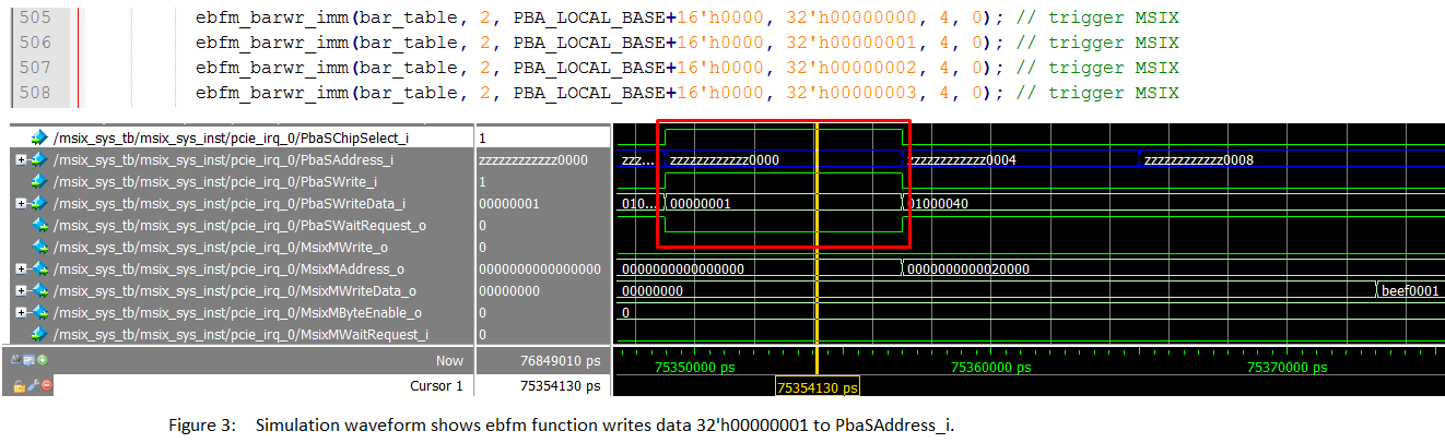
This example design shows the MSI-X interrupts simulation. It is based on Cyclone V device. MSI-X Design Example for Cyclone V
Follow the steps below to generate the testbench system to simulate the MSI-X design
1. Unzip the folder.
2. Open Quartus.
3. Open msix_sys.qsys.
4. Generate > Generate Testbench System: select "Standard" and the simulation model language.
5. Generate the testbench.
6. Replace ../msix_avmm_ref_design/msix_sys/testbench/msix_sys_tb/simulation/submodules/altpcietb_bfm_driver_avmm.v with ../msix_avmm_ref_design/altpcietb_bfm_driver_avmm.v.
7. Simulate using scripts.
a) Open ModelSim
b) cd <your project directory>/msix_avmm_ref_design/msix_sys/testbench/mentor
c) do msim_setup.tcl
d) ld_debug
e) do wave.do
e) run -all
8/83/Figure_1-2.png ( Figure 1-2.png - click here to view image )
e/e2/Figure_3.png ( Figure 3.png - click here to view image )
Avalon-MM-to-PCI Express Address Translation for 32-Bit Addressing
Note: Avalon-MM-to-PCI Express supports both 32- and 64-bit addresses.
If you select 64-bit addressing the bridge does not perform address translation.
However, when you specify 32-bit addresses, the Avalon-MM address of a received request on the TX Avalon-MM slave port is translated to the PCI Express address before the request packet is sent to the Transaction Layer.
The Avalon-MM-to PCIe Address (A2P) translation table is access through CRA interface.
Assume a design has 2 pages each with 1MB size (20 bits):
Bit[19:0] are passed through and become PCI Express address bits [19:0]. (due to the 1MByte page size -20 bits)
Bit[20] select the address translation table entry (0=select page#0, 1=select page#1)
Bit[31:21] select the TX slave module port from among other slaves connected to the same master by the system interconnect fabric. The decode is based on the base addresses assigned in Qsys. For setting up the translation table page 1:
At 0x1000 bit[1:0] set to 0x0 for 32 bit addressing.
At 0x1000 bit[31:21] is the host physical address.
At 0x1004 bit[31:0] is set to 0x00000000 (Writing all 0 to this address for 32 bits PCIe system.)
The steps to set up second address page is almost similar to page 1. (also applicable if there are more than 2 address pages)
To setup second page, use the PCIe CRA (Control Register Access) at offset 0x1008 - 0x100C.
At 0x1008 bit[1:0] set to 0x0 for 32 bit addressing.
At 0x1008 bit[31:21] is the host physical address.
At 0x100C bit[31:0] is set to 0x00000000 (Writing all 0 to this address for 32 bits PCIe system)
Community support is provided Monday to Friday. Other contact methods are available here.
Intel does not verify all solutions, including but not limited to any file transfers that may appear in this community. Accordingly, Intel disclaims all express and implied warranties, including without limitation, the implied warranties of merchantability, fitness for a particular purpose, and non-infringement, as well as any warranty arising from course of performance, course of dealing, or usage in trade.
For more complete information about compiler optimizations, see our Optimization Notice.