Intro to Altera SoC Devices for HW Developers Workshop - Configure the HPS
Success! Subscription added.
Success! Subscription removed.
Sorry, you must verify to complete this action. Please click the verification link in your email. You may re-send via your profile.
- Intel Community
- Intel Community Knowledge Base
- Product Support Forums Knowledge Base
- FPGA Knowledge Base
- FPGA Wiki
- Intro to Altera SoC Devices for HW Developers Workshop - Configure the HPS
Intro to Altera SoC Devices for HW Developers Workshop - Configure the HPS
- Subscribe to RSS Feed
- Mark as New
- Mark as Read
- Bookmark
- Subscribe
- Printer Friendly Page
- Report Inappropriate Content
Intro to Altera SoC Devices for HW Developers Workshop - Configure the HPS
Overview
In this section, you will launch Quartus and QSys and begin to build the SoC System. First you will configure the Hard Processor Subsystem. The HPS settings chosen in this lab are the setting which are compatible with the board you are using and the SW which is pre-installed on the SD card.
<<<<Click here to return to the previous section
Launch Quartus, Open the Project, and Launch QSys
1. Start Quartus II version 15.1 and open the project "DE0_NANO_SOC.qpf"
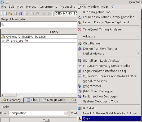
2. Launch QSys by selecting the "Tools" menu in Quartus then selecting "QSys"
Soc_hw_ws_files1.jpg (Click here for image)
3. Click "Close" in the "Initializating Completed" dialog box
Create Your Hard Process System in QSys
1. In the QSys "IP Catalog" window, expand "Processors and Peripherals", then expand "Hard Processor Systems"
2. Under "Hard Processor Systems", select "Arria V/Cyclone C Hard Processor System", then click the "Add..." button
Soc_hw_ws_files2.jpg (Click here for image)
3. You will first configure the interfaces between the FPGA and HPS. In the dialog box which appears, make the following changes from the defaults:
- Under "General", uncheck "Enable MPU standby and event signals"
- Under "AXI Bridges":
- Change "FPGA-to-HPS interface width:" to "128-bit"
- Change "HPS-to-FPGA interface width:" to "64-bit"
- Leave "Lightweight HPS-to-FPGA interface width:" at the default of "32-bit"
- Leave the defaults for all other settings.
- Under "FPGA-to-HPS SDRAM Interface":
- Change the width of "f2h_sdram0" to 256.
Soc_hw_ws_files3.jpg (Click here for image)
4. Next, you will configure the HPS peripheral pins to correctly pinout the peripherals needed for this design.
Once a peripheral is configured in the QSys GUI, Quartus will correctly assign pins without user intervention. This information is also transferred to the BSP Editor through the handoff files. The BSP Editor will use the handoff file information to generate a boot loader which will correctly configure the HPS pin muxes.
- Click the "Peripheral Pins" tab and make the following changes:
- Change "EMAC1 pin:" to "HPS I/O Set 0". This enables hard Ethernet MAC 1 in the HPS and pins it out correctly for the board
- Leave "EMAC1 mode:" at the default setting of "RGMII"
- Change "SDIO pin:" to "HPS I/O Set 0"
- Change "SDIO mode:" to "4-bit Data"
- Change "USB1 pin:" to "HPS I/O Set0:
- Leave "USB1 PHY interface mode:" at the default setting of "SDR with PHY clock output mode"
- Change "UART0 pin:" to "HPS I/O Set 0"
- Leave "UART0 mode:" at the default setting of "No Flow Control"
Soc_hw_ws_files4.jpg (Click here for image)
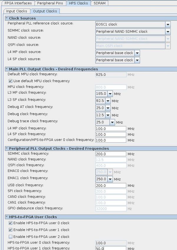
5. Now you will configure the clocking for the HPS. Again, the clock configuration information will be transferred to the BSP Editor. The BSP Editor will use the handoff file information to generate a boot loader which will correctly configure the HPS clocking.
- Click the "HPS Clocks" tab.
- Review the information in the "Input Clocks" tab. In this tab, the External Oscillator clock frequencies are specified and clocks sourced from the FPGA array can be enabled. For this lab, we will keep the default settings for the HPS input clocks.
- Click the "Output Clocks" tab. This selects HPS peripheral clock sources, sets Main PLL and Peripheral PLL output clock frequencies, and enables HPS to FPGA clock outputs.
- Scroll down to "HPS-to-FPGA User Clocks".
- Check "Enable HPS-toFPGA user 0 clock" and "Enable HPS-toFPGA user 1 clock"
- Change "HPS-toFPGA user 1 clock frequency:" to 50 MHz
Soc_hw_ws_files5.jpg (Click here for image)
6. Lastly we will HPS SDRAM Controller. Click the "SDRAM" tab in the HPS configuration GUI.
7. In the "PHY Settings" tab, make the following changes:
- Change the "Memory clock frequency" to 400.0 MHz:
- Change the "PLL reference clock frequency:" to 25.0 MHz
Soc_hw_ws_files6.jpg (Click here for image)
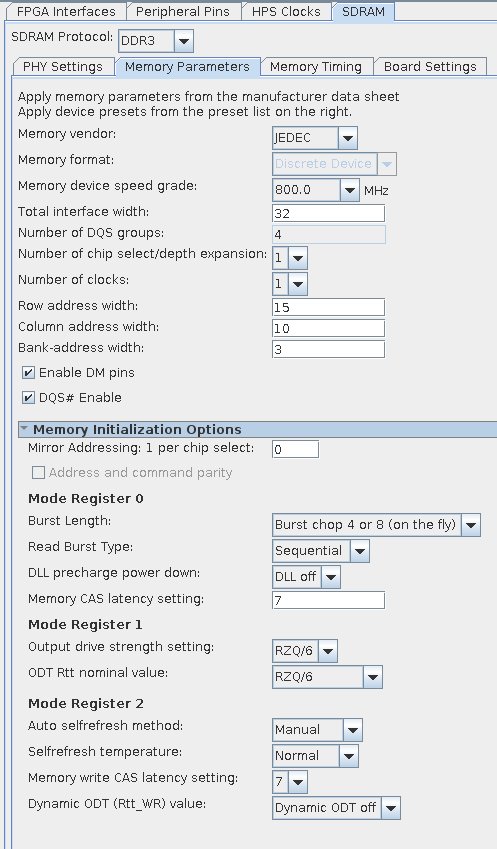
8. In the "Memory Parameters" tab, make the following changes:
- "Memory device speed grade:" 800 MHz
- "Total interface width:" 32
- "Row address width:" 15
- "Column address width:" 10
- "Bank-address width:" 3
- "Memory CAS latency setting:" 7
- "ODT Rtt nominal value:" "RZQ/6"
- "Memory write CAS latency setting:" 7
Soc_hw_ws_files7.jpg (Click here for image)
9. In the "Memory Timing" tab, make the following changes:
- iINIT: 500 us
- tMRD: 4 cycles
- tRAS: 35.0 ns
- tRCD: 13.75 ns
- tRP: 13.75 ns
- tREFI: 7.8 us
- tRFC: 300.0 ns
- tWTR: 4 cycles
Soc_hw_ws_files8.jpg (Click here for image)
10. In the "Board Settings" tab, you will keep the default settings.
Please note that you can use the default board settings because this development board uses the same layout as was used to generate the default settings. When building your own custom board, you will need to update the "Board Settings" tab with the values from your own board layout to ensure that Quartus properly closes timing on the SDRAM interface and to ensure that the SDRAM interface on your custom board works.
11. Click "Finish". You will see your HPS subsystem appear in the QSys "System Contents" window. You have now configured the HPS for the Atlas board.
12. So that you do not lose all of the work you just did, save your new QSys system. From the QSys File menu, click Save. Save the QSys system, in the same directory as the Quartus project files, as "soc_system.qsys". It is important that you use this name, as this is the name under which the QSys system is instantiated in the project's top-level Verilog file.
Note: As you build the system, errors will appear in the QSys "Messages" window. These errors will be resolved as you work through the lab.
You will now move on to the next section in which you will add FPGA peripherals to your system.
Community support is provided Monday to Friday. Other contact methods are available here.
Intel does not verify all solutions, including but not limited to any file transfers that may appear in this community. Accordingly, Intel disclaims all express and implied warranties, including without limitation, the implied warranties of merchantability, fitness for a particular purpose, and non-infringement, as well as any warranty arising from course of performance, course of dealing, or usage in trade.
For more complete information about compiler optimizations, see our Optimization Notice.