Measuring Channel Signal Integrity
Success! Subscription added.
Success! Subscription removed.
Sorry, you must verify to complete this action. Please click the verification link in your email. You may re-send via your profile.
- Intel Community
- Intel Community Knowledge Base
- Product Support Forums Knowledge Base
- FPGA Knowledge Base
- FPGA Wiki
- Measuring Channel Signal Integrity
Measuring Channel Signal Integrity
- Subscribe to RSS Feed
- Mark as New
- Mark as Read
- Bookmark
- Subscribe
- Printer Friendly Page
- Report Inappropriate Content
Measuring Channel Signal Integrity
This topic explains how to measure and enter the channel Signal integrity for Stratix V, Arria V and Cyclone V devices.
As the datarates of external memory interface go up, it is required that proper channel singal integrity measurement are done and entered in the megawizard GUI. Measuring the actual channel loss during the layout process points to the margins available for the memory interface.
Objective
The purpose of this topic is to show why channel loss measurement are important and provide a guideline on how to carry out the measurements.
What do we mean by Channel Signal Integrity?
Channel signal integrity is a measure of the distortion of the eye due to intersymbol interference or crosstalk or other effects. While the Quartus timing model includes some channel uncertainty, you will need to perform your channel signal integrity simulations and enter the extra channel uncertainty, as compared to the reference eye, into the MegaWizard GUI.
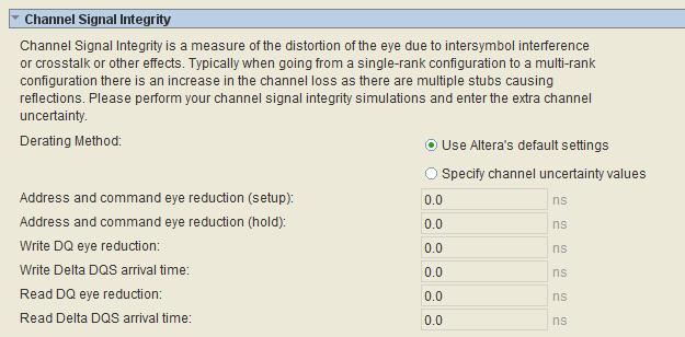
Starting with Quartus Version 13.1 you will see following section in the board settings tab for 28 nm devices.
Quartus_screen.jpg (Click here for image)
Why do we need accurate Channel Signal Integrity information?
While calculating the available timing margins, default values for Channel loss (or eye reduction) is taken into consideration. However, these default values are based on measurement that we do in our characterization boards which may not accurately represent the channel loss that you have in your system. If channel loss for your system is different than default value then the timing margin available to you will vary accordingly. For example if your channel loss is more than the default channel loss and if you don’t enter these accurate numbers in the megawizard GUI then your available timing margins for the entire system are lower than what Quartus compilation might show you. Which might mislead you to think that you have good timing margin; while in reality, you may need to tweak your board design to get improved Channel Signal Integrity.
Recommended Flow
When you have the first draft of your memory interface layout, Altera recommends that you perform board level simulation to calculate various Channel Signal Integrity parameters. The later part of the section explains how to calculate the Channel Signal Integrity parameter with a board simulation example.
Once you have the fairly accurate Channel Signal Integrity numbers, enter these numbers in the megawizard GUI along with accurate ‘Set up and hold derating’ and accurate ‘Board Skews’. Generate and IP which represents your system and run a Quartus compilation.
If you see negative timing margins then you need to change your layout accordingly to make improvements on trace length mismatch or ISI or crosstalk. Recalculate accurate ‘Channel Signal Integrity’, ‘Setup and Hold Derating’ and ‘Board Skew’ parameters. Regenerate and recompile the design. Repeat this step until you see positive timing margins.
Here is a flow chart that summarizes recommended flow.
Flow.jpg (Click here for image)
Tweaking your layout
Here are few things you should consider while tweaking your layout in order to get better signal integrity. * Board Skew: Make sure the skew within different data groups of the memory interface are well matched. EMIF Handbook chapter 4 mentions some of these guidelines.
http://www.altera.com/literature/hb/external-memory/emi_plan_board_ddr2.pdf
- ISI/Crosstalk: EMIF Handbook chapter 4 mentions some of these guidelines.
http://www.altera.com/literature/hb/external-memory/emi_plan_board_ddr2.pdf
- Also,check with your memory vendors to see if they have any reuqirements on how traces should be laid out on the board.
Please note that below list is no way a comprehensive list or hadened guidelines. Users should take them as recommendations and apply them along with best practices of the board layout design.
General Concept of Measuring Channel Signal Integrity
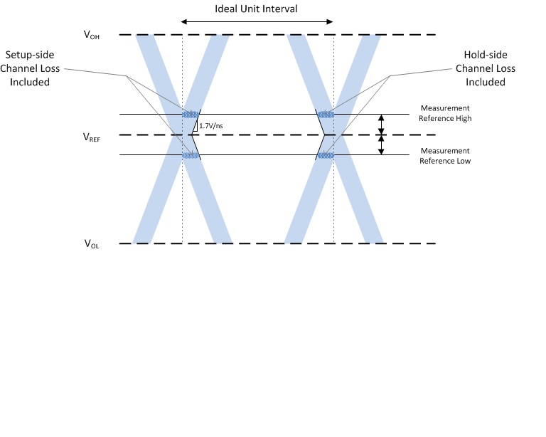
To measure channel signal integrity you need to measure the channel loss for various signals. For a particular signal or signal trace, channel loss is defined as loss of the eye width at +/- VIH(ac and dc) +/- VIL(ac and dc). VIH/VIL above or below Vref is used to align with various requirements of the Quartus timing model for memory interfaces.
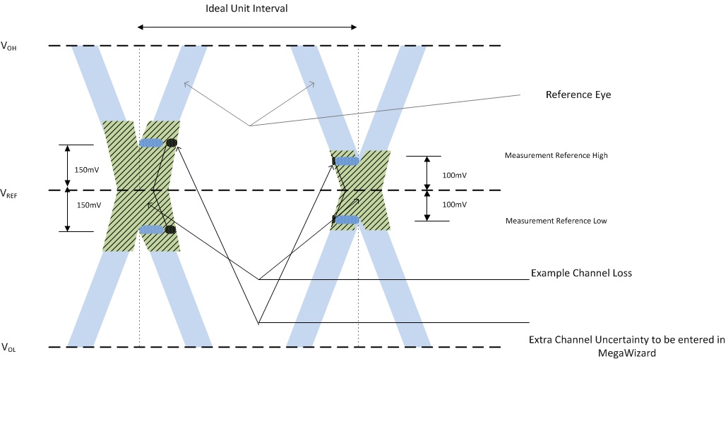
One such example is show in Figure 1 below. In the example reference eye diagram the channel loss on the setup- or leading-side of the eye is equal to the channel loss on the hold- or lagging-side of the eye, but it does not necessarily have to be that way. Since Altera’s calibrating PHY will calibrate to the center of the read and write eye, the Board Settings Panel has input for the total extra channel loss for Write DQ and Read DQ; however, for address/command signals which are not-calibrated, the Board Settings Panel supports entering non-equal setup- and hold-side channel losses so that Quartus can place the clock statically within the center of the address/command eye.
As explained earlier, a certain amount of channel loss is already included in Quartus timing calculation. Table below shows the default values for various signals.
| Setup (ps) | Hold (ps) | Total (ps) | |
|---|---|---|---|
| A/C | 250 | ||
| Write | 350 | ||
| Read Capture | 225 |
If your measured channel loss value is more than the default values entered than you should enter the difference in the megawizard GUI for channle loss. If your measured channel loss is less than default values then you should enter the negative difference.
General_Concept.jpg (Click here for image)
Measuring voltage level at FPGA (during Read)
During read, it is recommended that you measure at the input of the ‘Input Buffer’. In other words you need measure the input voltage at FPGA die and not at the FPGA pin. Measuring at the FPGA pin may end up in un-necessary reflection of the measured trace.
Input buffer of 28 nm device shows that the VIH and VIL is measured at +/- 70 mV with reference to Vref. For example; for 1.5 V DDR3 protocol the Vref is defined at Vcc/2. In this case the channel loss should be measured at (750 mV + 70 mV) 820 mV and (750 mV – 70 mV) 680 mV.
You may need to make the necessary changes to the IBIS file to measure voltage at the die. Same way you may need to manually change the IBIS file to measure the VIH and VIL at +/- 70 mV.
Measuring voltage level at Memory (during Write)
Writes should be measured at the VIH (ac and dc) and VIL (ac and dc) as mentioned in the Memory datasheet. Please make sure that you that setup time measurement voltage level is consistent with the setup time values which you entered in the ‘Timing Parameter’ tab of Megawizard.
For example, the setup time requirement for AC150 is different from setup time requirement for AC135 for DDR3 800 MHz. If you are entering AC150 setup value in the ‘Timing Parameter’ tab of the megawizard GUI then you should use 150 mV as VIH(ac) and VIL(ac)
Measure Address Command Eye Reduction (setup and hold)
Figure 4 shows the reference eye diagram for the address/command signals. The Board Settings Panel supports entering the extra channel loss as compared to the reference eye diagram separately on the setup-side and hold-side. The channel loss as compared to the ideal unit interval should be measured at Vref +/- VIH(ac and dc) and +/- VIL(ac and dc) as a result of requirements in the Quartus timing model. Note that other aspects of the timing model, such as the slew-rate derating explained above, are aligned with the JEDEC specified VIH/VIL values. Altera includes 125ps of channel loss on the setup side and 125ps of channel loss on the hold side. Any extra channel loss on your board should be entered into the Board Settings Panel.
For example if your board had 170ps of channel loss on the setup side and 120ps of channel loss on the hold side of the address/command eye, as shown in Figure 4, you should enter (170 ps - 125 ps) 45ps and (120 ps - 125 ps) -5ps respectively in the “Address and command eye reduction (setup)” and “Address and command eye reduction (hold)” input boxes in the Board Settings Panel.
AC_write.jpg (Click here for image)
Measure Write DQ eye reduction
Figure 5 shows the reference eye diagram for the write DQ signals. The Board Settings Panel asks for the total channel loss as compared to the reference eye diagram. The channel loss as compared to the ideal unit interval should be measured at Vref +/- VIH/VIL as mentioned in the memory datasheet. Altera includes 338ps of channel loss; any extra channel loss on your board should be entered into the Board Settings Panel.
AC_write.jpg (Click here for image)
For example if your board had 350ps of channel loss you should enter 12ps in the “Write DQ eye reduction” input box in the Board Settings Panel, as 338ps has already been included by Altera. Alterantively if your write channel loss is less than default write channel loss value; for example 300 ps. Then you should enter -38ps as your 'Write DQ eye reduction'.
Measure Read eye DQ reduction
Figure 6 shows the reference eye diagram for the read DQ signals. The Board Settings Panel asks for the total channel loss as compared to the reference eye diagram. The channel loss as compared to the ideal unit interval should be measured at Vref +/- 70mV. Altera includes 218ps of channel loss; any extra channel loss on your board should be entered into the Board Settings Panel.
For example if your PCB has 225ps of channel loss, you should enter 7ps in the “Read DQ eye reduction” input box in the Board Settings Panel. If your PCB has 210 ps of channel lost you should enter -8ps in the “Read DQ eye reduction” input box in the Board Settings Panel
Read_side.jpg (Click here for image)
Mesure Read/Write Delta DQS arrival time
For write and read timing analysis, the Board Settings Panel also allows for entering any extra uncertainty on DQS as compared to the reference DQS signal, due to non-ideal effects as shown in Figure 7. Generally because DQS is a 1/0/1/0 pattern there is not as much channel loss compared to DQ, but because of cross-talk and other effects there may be some variation in DQS at the 0V differential point (which is nominally at VREF). You should perform a channel simulation of DQS and any variation in DQS crossing the 0V differential point should be entered in the “Write Delta DQS arrival time” input box.
DQS.jpg (Click here for image)
Measuring Channel Signal Integrity Example
There are several ways to measure Channel Signal Integrity. The purpose of below mentioned document is to demonstrate a simple and fairly accurate way to calculate Channel Signal Integrity numbers for your PCB.
https://www.intel.com/content/dam/altera-www/global/en_US/uploads/6/6b/Channel_SI_Example.zip
Above mentioned zip file is a word document which is a step by step guide on how to measure channel signal integrity using DDRx Wizard of Mentor Graphics BoardSim simulator.
Here are the supporting file that you need to follow the step by step instruction given in the Channel_SI_Example.docx.
- Altera SV Devkit board file(HYP file) in Hyperlynx readable format. Copy this file in folder where you want create the Hyperlynx simulation project.
https://www.intel.com/content/dam/altera-www/global/en_US/uploads/9/9f/S5GX_PCIE_E.zip
- IBIS model for the FGPA used on the Devkit
https://www.intel.com/content/dam/altera-www/global/en_US/uploads/8/86/Ddr3_x72_devkit.zip
- IBIS model for the memory device used on the devkit.
https://www.intel.com/content/dam/altera-www/global/en_US/uploads/5/52/V89c.zip
- FPGA timing file for the DDRx Wizard.
https://www.intel.com/content/dam/altera-www/global/en_US/uploads/5/50/Ddr3_800.zip
Note: Please download the IBIS file in the MentorGraphics\9.0HL\SDD_HOME\hyperlynx\Libs folder.
Community support is provided Monday to Friday. Other contact methods are available here.
Intel does not verify all solutions, including but not limited to any file transfers that may appear in this community. Accordingly, Intel disclaims all express and implied warranties, including without limitation, the implied warranties of merchantability, fitness for a particular purpose, and non-infringement, as well as any warranty arising from course of performance, course of dealing, or usage in trade.
For more complete information about compiler optimizations, see our Optimization Notice.