On-Board USB-Blaster II
Success! Subscription added.
Success! Subscription removed.
Sorry, you must verify to complete this action. Please click the verification link in your email. You may re-send via your profile.
- Intel Community
- Intel Community Knowledge Base
- Product Support Forums Knowledge Base
- FPGA Knowledge Base
- FPGA Wiki
- On-Board USB-Blaster II
On-Board USB-Blaster II
- Subscribe to RSS Feed
- Mark as New
- Mark as Read
- Bookmark
- Subscribe
- Printer Friendly Page
- Report Inappropriate Content
On-Board USB-Blaster II
This page is created to host unpublished documentation to support On-Board USB-Blaster™ II for the Altera Stratix V GX FPGA development board to be released in early November 2011. Please check back soon for updates and links to the published development board manuals.
The Stratix V FPGA Development Board
The Stratix V FPGA development board includes an On-Board USB-Blaster II interface. This circuit is compatible with USB 2.0 high speed (480Mbit/s) connections on the host. It provides two independent interfaces:
- A JTAG interface
- A fast parallel interface designed for use with the System Console
The Stratix V GX FPGA development board includes integrated On-Board USB-Blaster II circuitry for FPGA programming. However, for the host computer and board to communicate, you must install the USB-Blaster driver on the host computer. Installation instructions for the USB-Blaster driver for your operating system are available on the Altera website. On the Altera Programming Cable Driver Information page of the Altera website, locate the table entry for your configuration and click the link to access the instructions.
The JTAG interface is supported by the ACDS tools (Quartus programmer, SignalTap, System Console, Nios II debugger etc.) in the same way as earlier USB-Blaster but operates at a higher speed. For details on the JTAG chain, refer to the Stratix V GX FPGA development board documentation: Stratix V GX FPGA Development Board Reference Manual and the Stratix V GX FPGA Development Kit User Guide.
The System Console USB interface provides a fast parallel interface which can be used in two ways: (1) It can be used with Altera supplied soft logic to provide a System Console master for debug access, and with a bit more work, and (2) it can be used as a transparent pipe.
Using the System Console USB Interface
The USB Debug Master Bridge core provides a connection between System Console and a QSYS or SOPC builder system via the On-Board USB-Blaster™ II fast parallel interface. The System Console can initiate Avalon Memory-Mapped (Avalon-MM) transactions by sending encoded streams of bytes through the USB endpoints. The core supports reads and writes, but not burst transactions.
The USB Debug Master Bridge is QSYS-ready and integrates easily into any QSYS or SOPC Builder-generated systems.
Parameters and Interfaces
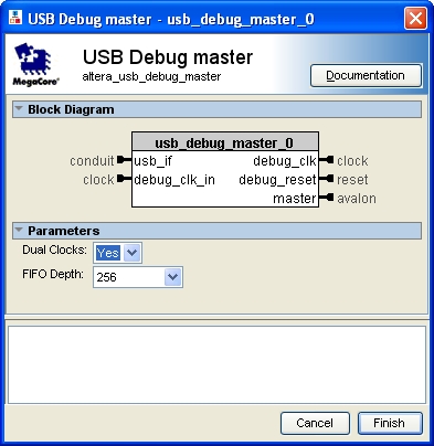
The following figure shows the parameterization interface provided by the USB Debug Master component.
USB_Debug_master_dialog.jpg (Click here for image)
The usb_if interface is used to communicate with the USB interface. You should connect this interface to the USB_ pins on the FPGA as shown in the following table.
| Name | Direction | Pin | Notes |
| usb_clk | input | AV28 | 48MHz |
| usb_reset_n | imput | H34 | |
| usb_dat[7:0] | bidir | A35, C34, A36, A37, E32, F32, G33, G32 | |
| usb_full | output | N34 | |
| usb_empty | output | P34 | |
| usb_wr_n | input | J33 | |
| usb_rd_n | input | K33 | |
| usb_oe_n | input | E33 | |
| usb_addr | birdir | G34, K34 | Reserved |
| usb_scl | bidir | J34 | |
| usb_sda | bidir | F33 |
The master interface on the component should be connected to the slaves you want to access from the host. The debug_clk and debug_reset interfaces provide a clock and reset for this interface.
The Dual Clocks parameter controls the clocking of the component. If the parameter is set to "No" then the whole component runs from the 48MHz clock provided by the USB interface, the debug_clk interface is also driven from this 48MHz clock.
If the Dual Clocks parameter is set to "Yes" then the component enables internal clock crossing circuitry. All user visible interfaces run from a clock provided by the user through the debug_clk_in interface - this clock is also available as an output on the debug_clk interface.
The component contains two FIFOs, one for use in the host to target direction and one in the target to host direction. The FIFO Depth parameter controls the number of bytes in each of these FIFOs. With some workloads larger FIFOs will enable higher performance.
Using the Master
Once you have connected the component and programmed your board you can use the System Console software (version 11.0 sp1 or later) to access the debug master. See the System Console documentation for further details.
Using the System Console USB Interface Standalone
If you do not want to use System Console and the altera_usb_debug_master to debug your system then the interface can be used standalone. You will need to write your own hardware to communicate within the FPGA and your own software to drive the interface.
This task is considerably harder than using the provided soft cores and software. The amount of support available from Altera will be limited if you are taking this path.
The On-Board USB-Blaster II Hardware Interface
The hardware interface between the On-Board USB-Blaster II and the FPGA is shown in table above.
The System Console interrogates the hardware using the I2C management interface to look for System Console compatible soft logic. You should leave the USB_SCL and USB_SDA lines unconnected so that SystemConsole will not find this logic and will therefore not use the interface.
Your soft logic should be clocked by the USB_CLK pin which will provide a 48MHz clock when the USB interface is connected and configured. All pins (apart from reset) on this interface operate synchronously to the rising edge of this clock.
Host software can control the setting of the USB_RESETn pin using USB control messages. Your logic would normally use this pin as an active low reset. Note that this pin is not synchronized to USB_CLK so your soft logic will need appropriate synchronization.
The USB_DATA pins are the data bus over which data to/from the host will be transmitted. You must configure this to be an input when USB_OEn is high, and should drive data out of it when USB_OEn is low. The On-Board USB-Blaster II will deassert USB_OEn one cycle before it starts driving data to provide turnaround time.
A scheduler within the On-Board USB-Blaster II monitors the USB_FULL and USB_EMPTY pins from the FPGA and the status of the USB FIFOs. When it is able to transfer data it will use the USB_WRn and USB_RDn pins to transfer data.
The scheduler will attempt to optimize transfer bandwidth by transferring data on consecutive cycles if data is available, then it will keep USB_WRn or USB_RDn low for multiple cycles, transferring a different data byte on each cycle.
You should drive USB_FULL low if there is space in the FPGA for host to target data (resulting from USB OUT packets). When USB_FULL is low the USB_WRn signal will be used to write data into the target one byte at a time.
If there is no space in the FPGA for host to target data then you must drive USB_FULL high to stop the flow of data. The On-Board USB-Blaster II may send data for up to two clocks after you set USB_FULL high so you should connect it to a signal which indicates that your input FIFO (for example) has two bytes or fewer remaining.
If your soft logic has no data to transfer to the host it should drive USB_EMPTY high. If you drive USB_EMPTY low then the On-Board USB-Blaster II will read data from your logic using the USB_RDn signal.
When your logic has no more data to transfer it should drive USB_EMPTY high again. Note that due to pipelining delays the On-Board USB-Blaster II may read on cycles when USB_EMPTY is high. The data read on these cycles will be discarded and not transferred to the host.
The On-Board USB-Blaster II Software Interface
On Windows you should use the INF files provided with the ACDS software to load the winusb kernel mode drivers for the On-Board USB-Blaster II. You must also run the Altera JTAG Server so that it can program the firmware for the device. One easy way to trigger a firmware download (if required) is to run the jtagconfig command and discard its output.
Please refer to Microsoft documentation for instructions on how to obtain winusb.dll and how to use the WinUSB drivers. The Altera supplied INF files bind the System Console interface to GUID {09FB6010-0001-1000-0000-00B0D03D3169}. You should search for this using the standard Microsoft SetupDi functions.
On Linux no kernel mode drivers are required. You should use a library such as libusb to locate and open the hardware. Documentation on libusb is available from http://www.libusb.org/ .
You will need to claim interface 1 on the hardware once you have opened it. Claiming other interfaces on the hardware will prevent jtagd from operating.
Once you have located and found the hardware then you should parse the configuration descriptors to discover which endpoints are available on interface 1.
The first OUT endpoint on this interface (usually endpoint 2) is used to send data from host to target. The packet boundaries on this interface are ignored by the hardware.
The first IN endpoint on this interface (usually endpoint 0x86) is used to receive data from the target. If your hardware provides data at a high enough rate then the On-Board USB-Blaster II will send maximum sized packets to the host. If no data is received from the FPGA for approximately 2µs then a partial packet will be sent to the host.
Your software can control the USB_RESETn signal and flush buffers within the On-Board USB-Blaster II by issuing a control transfer through endpoint 0 with type 0x41, request 0x80, index 0 and length 0.
- Bit 0 of the value field controls the USB_RESETn signal.
- If bit1 of the value field is 1 then the internal FIFOs within the hardware will be flushed
- Bits 7:2 of the value field are reserved and should be written as 0
The remaining endpoints within this interface are reserved and should not be used by your software.
Community support is provided Monday to Friday. Other contact methods are available here.
Intel does not verify all solutions, including but not limited to any file transfers that may appear in this community. Accordingly, Intel disclaims all express and implied warranties, including without limitation, the implied warranties of merchantability, fitness for a particular purpose, and non-infringement, as well as any warranty arising from course of performance, course of dealing, or usage in trade.
For more complete information about compiler optimizations, see our Optimization Notice.