Timing Constraints
Success! Subscription added.
Success! Subscription removed.
Sorry, you must verify to complete this action. Please click the verification link in your email. You may re-send via your profile.
Timing Constraints
- Subscribe to RSS Feed
- Mark as New
- Mark as Read
- Bookmark
- Subscribe
- Printer Friendly Page
- Report Inappropriate Content
Timing Constraints
This page should help you understand what timing constraints are and how to apply them. This page will give you an overview of what synchronous and asynchronous signals are and the most important commands to constrain a design.
What are timing constraints?
During the synthesis of your FPGA design a tool called TimeQuest will be called by Quartus II. This tool will read in timing constraints files. The timing constraints files describe the timing for your FPGA, for example the target frequency of your FPGA and the timing to external peripherals. This constraint file uses the Synopsys timing constraints description language. TimeQuest will then calculate the timing of the internal FPGA signals and compare these timings to the required timing given by the timing constraints files.
Synchronous signals
Synchronous signals change their values synchronously to a clock signal. The signal can either change at the rising or falling edge of clock signal. The data gets latched also at either the rising or falling edge of the clock. FPGA internal registers can only launch/latch a signal at either the falling or rising edge of the clock. It's not possible to launch/latch a signal at both the falling and rising edge of the clock. Normally a FPGA provides some special circuitry for external DDR signal which can launch/latch data at both the rising and falling edge of the clock. These external DDR signals are the only signals which can be launched/latched at both the rising and falling edge of the clock.
Example for data launched at the rising edge of the clock - 7/7c/Data_sdr_launch_rising_edge.png
Example for data launched at the falling edge of the clock 9/98/Data_sdr_launch_falling_edge.png
Example for data launched at both the rising and falling edge of the clock - 8/80/Data_ddr.png
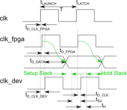
Setup/hold and slack
Setup time describes the time the signal has to be stable before the latch edge and hold time describes the time the signal has to be stable after the hold edge.
Slack describes by how much the setup and hold times are overfulfilled. If the slack is positive that means that the timing requirements are overfulfilled if the slack is negative it means that the timing requirements are not met.
d/d3/Setup_hold_slack.png -Setup, hold and slack relationships
This figure shows the relationship between the setup and hold relationships and the corresponding slack times. The data is launched at the first register and latched at the second register. Launch and latch clocks are edge aligned and have the same frequency. There is some routing delay for the data from the first to the second register. The second register does have a hold and a setup requirement which means that the data has to be stable a certain amount of time before and after the latch edge. The slack times are calculated like this:
setup slack = data needed setup time - data stable time
hold slack = data change time - data needed hold time
A positive slack means that the timing requirements are met and a negative slack means that the timing requirements are not met.
Clocks
In a synchronous design you need to define the clocks used in the design. There are three types of clocks you can define:
Clocks at FPGA clock input PIN
Virtual clocks which are used to describe the clocking of FPGA external registers (external device registers)
Generated clocks which are derived other clocks
The command for creating clocks at FPGA input pins and virtual clocks is the same. The only difference is that you don't specify a FPGA input pin for virtual clocks. Because of this they are both listed under create_clocks.
Overview of different clock types in a FPGA system
create_clocks
These clocks are defined by the create_clock command. Created clocks are the base clocks of the system and are the clocks which generated clocks derive from. With this command you can specify the clock frequency and phase of the clock.
Clocks at input pins
You create a FPGA base clock when you specify an input port signal with the create_clock command.
Virtual clocks
The clocks are called virtual because they are not connected to a clock input pin of the FPGA. You need virtual clocks if you have connected synchronous peripherals to the FPGA which are not clocked by the FPGA. With a virtual clock you can describe the clock relationship between the FPGA clock and the external device clock.
Generated clocks
The create_generated_clock command creates clocks which are derived from created clocks. Such clocks could for example be clocks generated by PLLs (clocks generated by PLLs can be constrained manually but it is recommended to let TimeQuest automatically constrain these clocks via the derive_pll_clocks command).
derive_pll_clocks
The derive_pll_clocks automatically generates clock constraints for clocks generated by PLLs. If you use PLLs in your design it is recommended to use this command to automatically constrain the clocks generated by PLLs. You can also constrain the generated clocks manually but you have to remember to update the .sdc constraints if you change the PLL settings.
derive_clock_uncertainty
The derive_clock_uncertainty command automatically generate clock uncertainty values for FPGA clock signals. Basically clock uncertainty is the jitter of a clock. This command should always be used in your timing constrain file.
set_clock_groups
By default TimeQuest assumes that there is a relationships between all clocks and thus examines all paths between the clocks. With the set_clock_groups you can tell TimeQuest that it should ignore paths for clocks which are in different groups. You should be really sure what you want to do if you use this command!
This is an example if you want to cut the paths between some clocks:
set_clock_groups -exclusive -group [get_clocks {enet_rx_clk_125mhz virtual_enet_rx_clk_125mhz}] -group [get_clocks {enet_rx_clk_25mhz virtual_enet_rx_clk_25mhz}]
In this example enet_rx_clk_125mhz and virtual_enet_rx_clk_125mhz would be in the same clock group. Also enet_rx_clk_25mhz and virtual_enet_rx_clk_25mhz would be in the same clock group. The paths between the 125 MHz clocks and the 25 MHz clocks would be cut.
Example for clock mux
TimeQuest Clock Multiplexer Examples
Input/output constraints
If you have defined the input clocks TimeQuest can analyze the timing for data transfers within the FPGA. If you have external devices connected to the FPGA you need to specify the timing for these devices so that TimeQuest is able to analyze these data paths as well. TimeQuest needs to know for example the external clock and data delays and the tSU, tH, tCO(max) and tCO(min) of the external devices.
What TimeQuest already knows
If the FPGA input clocks are constrained the TimeQuest can calculate the FPGA internal data delays from the input and output ports. TimeQuest also knows the clock edge at which the data gets launched/latched inside the FPGA. So you don't have to describe these parameters as TimeQuest will automatically do that for you.
What TimeQuest needs to know
TimeQuest needs to know the external delays of the clock and the data signals and the clock edge at which the data gets launched/latched. These are the parameters which you have to describe for TimeQuest to be able to fully check the timing requirements of your design.
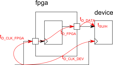
Output constraints
Output data signals can be constrained using the set_output_delay command. You need to set a value for the minimum and the maximum output delays. If you look at the following figure:
Timing diagram for data output from FPGA- 9/99/Fpga_data_output_setup_hold_relationship_timing.png
Schematic for clock/data path for data output from FPGA - 9/9c/Fpga_data_output_setup_hold_relationship_data_path.png
you get the following relationships for the clock delays:
tD_CLK(max) = tD_CLK_DEV(max) - tD_CLK_FPGA(min)
tD_CLK(min) = tD_CLK_DEV(min) - tD_CLK_FPGA(max)
Maximum output delay
The maximum output delay is equal to the minimal setup slack. The minimal setup slack is calculated in the following steps:
Latest data arrival:
tLAUNCH + tD_CLK_FPGA(max) + tD_FPGA(max) + tD_DATA(max)
Data needed:
tLATCH + tD_CLK_DEV(min) - tSU_DEV
The relation between tLATCH and tLAUNCH ist determined by the chosen multicycle constraint (in this example the default relationship for tLATCH and tLAUNCH was used).
Minimal setup slack:
Minimal setup slack = Data needed - Latest data arrival
<=> tLATCH + tD_CLK_DEV(min) - tSU_DEV - (tLAUNCH + tD_CLK_FPGA(max) + tD_FPGA(max) + tD_DATA(max))
<=> tLATCH - tLAUNCH - tD_FPGA(max) + tD_CLK_DEV(min) - tD_CLK_FPGA(max) - tD_DATA(max)- tSU_DEV
<=> tLATCH - tLAUNCH - tD_FPGA(max) - (tD_DATA(max)+ tSU_DEV - tD_CLK(min))
<=> tLATCH - tLAUNCH - tD_FPGA(max) - maximum_output_delay
Or to describe the maximum output delay in another way:
max output delay = device tSU_DEV + sum of all max buffer delays on data path - sum of all min buffer delays on clock path
Minimum output delay
The minimum output delay is equal to the minimal hold slack. The minimal hold slack is calculated in the following steps:
Earliest data change:
tLAUNCH + T + tD_CLK_FPGA(min) + tD_FPGA(min) + tD_DATA(min)
Because the data in this example is launched at the rising edge of the clock the next time the data changes is after one clock period T after tLAUNCH.
Data hold time:
tLATCH + tD_CLK_DEV(max) + tH_DEV
This example also uses the default multicycle constraints. If you want to change the latch clock edge for the hold timing analysis to another time than tLAUNCH + T you need to modify the multicycle clock constraint.
Minimal hold slack:
Minimal hold slack = Earliest data change - Data hold time
<=> tLAUNCH + T + tD_CLK_FPGA(min) + tD_FPGA(min) + tD_DATA(min) - (tLATCH + tD_CLK_DEV(max) + tH_DEV)
<=> tLAUNCH - tLATCH + T + tD_FPGA(min) + tD_DATA(min) + tD_CLK_FPGA(min) - tD_CLK_DEV(max) - tH_DEV
<=> tLAUNCH - tLATCH + T + tD_FPGA(min) + tD_DATA(min) - (tD_CLK_DEV(max) - tD_CLK_FPGA(min)) - tH_DEV
<=> tLAUNCH - tLATCH + T + tD_FPGA(min) + tD_DATA(min) - tD_CLK(max) - tH_DEV
<=> tLAUNCH - tLATCH + T + tD_FPGA(min) + minimum_output_delay
or to describe the maximum output delay in another way:
min output delay = -device tH_DEV + sum of all min buffer delays on data path - sum of all max buffer delays on clock path
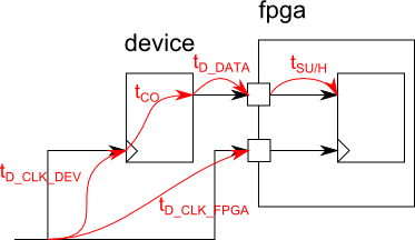
Input constraints
Input data signals can be constrained using the set_input_delay command. You need to set a value for the minimum and the maximum input delays. If you look at the following figure:
Timing diagram for data input to the FPGA - 3/3c/Fpga_data_input_setup_hold_relationship_timing.png
Schematic for clock/data path for data input to the FPGA - 6/66/Fpga_data_input_setup_hold_relationship_data_path.png
you get the following relationships for the clock delays:
tD_CLK(max) = tD_CLK_FPGA(max) - tD_CLK_DEV(min)
tD_CLK(min) = tD_CLK_FPGA(min) - tD_CLK_DEV(max)
Maximum input delay
The maximum input delay is equal to the minimal setup slack. The minimal setup slack is calculated in the following steps:
Latest data arrival:
tLAUNCH + tD_CLK_DEV(max) + tCO_DEV(max) + tD_DATA(max)
Data needed:
tLATCH + tD_CLK_FPGA(min) - tSU_FPGA
Minimal setup slack:
Minimal setup slack = Data needed - Latest data arrival
<=> tLATCH + tD_CLK_FPGA(min) - tSU_FPGA - (tLAUNCH + tD_CLK_DEV(max) + tCO_DEV(max) + tD_DATA(max))
<=> tLATCH + tD_CLK_FPGA(min) - tSU_FPGA - tLAUNCH - tD_CLK_DEV(max) - tCO_DEV(max) - tD_DATA(max)
<=> tLATCH - tLAUNCH - tSU_FPGA - tCO_DEV(max) - tD_DATA(max) + tD_CLK_FPGA(min) - tD_CLK_DEV(max)
<=> tLATCH - tLAUNCH - tSU_FPGA - (tCO_DEV(max) + tD_DATA(max) - tD_CLK(min))
<=> T - tSU_FPGA - maximum_input_delay
or to describe the maximum input delay in another way:
max output delay = device tCO_DEV + sum of all max buffer delays on data path + sum of all max buffer delays on clock path
Minimum input delay
The minimum input delay is equal to the minimal hold slack. The minimal hold slack is calculated in the following steps:
Earliest data change:
tLAUNCH+ T + tD_CLK_DEV(min) + tCO_DEV(min) + tD_DATA(min)
Data hold time:
tLATCH + tD_CLK_FPGA(max) + tH_FPGA
Minimal hold slack:
Minimal hold slack = Earliest data change - Data hold time
<=> tLAUNCH + T + tD_CLK_DEV(min) + tCO_DEV(min) + tD_DATA(min) - (tLATCH + tD_CLK_FPGA(max) + tH_FPGA)
<=> tLAUNCH + T - tLATCH - tH_FPGA + (tCO_DEV(min) + tD_DATA(min) - (tD_CLK_FPGA(max) - tD_CLK_DEV(min)))
<=> tLAUNCH + T - tLATCH - tH_FPGA + (tCO_DEV(min) + tD_DATA(min) - tD_CLK(max))
<=> tH_FPGA + minimum_input_delay
or to describe the maximum output delay in another way:
min output delay = min device tCO_DEV + sum of all min buffer delays on data path + sum of all min buffer delays on clock path
Pitfalls
Don't use the set_max_delay and set_min_delay command unless you really know what they do! These two commands can result in some unwanted side effects which are described in the TimeQuest User Guide, V 1.1 on page 65.
Multicycles
With multicylces you can define the launch and latch edges for setup and hold analysis. For this you need to understand the default setup and hold relationships first.
Default setup/hold launch/latch edges relationships
If you don't change the multicycles constraint TimeQuest analyzes the flollowing setup and hold times:
Minimum setup time: Minimum time between launch and latch edge with the following conditions:
tlatch - tlaunch > 0 s
min(tlatch - tlaunch)
Minimum hold time: Minimum time between launch and latch edge with the following conditions:
tlaunch - tlatch >= 0 s
min(tlaunch - tlatch)
Example
Example for default setup and hold relationships
The latch clock frequency in this example is 2/5 of the launch clock frequency. The green arrow denotes the clock edges which fulfill the minimal setup time and the red arrow denotes the clock edges which fulfill the minimal hold time.
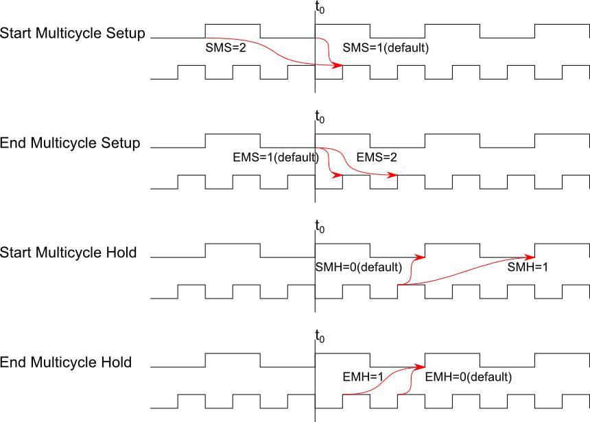
Understanding start/end setup/hold multicycle constraints
When you use multicycles constraints you can tell TimeQuest the times the data changes and when the data gets latched. For this you need to use the set_multicycle_path constraint. With this command you can change the launch and latch edge for setup and hold analysis. The next figure gives you an overview of what happens when you change the values. The default values denote the value TimeQuest uses if you don't specify any multicycle constraints.
c/ce/Multicycle_constraints.jpg - Multicycle constraints change setup/hold start/end values
The setup and hold relationships are dependent though: The setup constraint gets analyzed always before the hold requirement. This means that:
set_multicycle_path -from [get_cells {inst1}] -to [get_cells {inst2}] -setup -start 2
set_multicycle_path -from [get_cells {inst1}] -to [get_cells {inst2}] -hold -start 0
is equal to writing:
set_multicycle_path -from [get_cells {inst1}] -to [get_cells {inst2}] -hold -start 0
set_multicycle_path -from [get_cells {inst1}] -to [get_cells {inst2}] -setup -start 2
This is important because the hold constraint is always in relation to the setup constraint. If you change the setup edge for analysis the hold edge will follow. If you change the start setup multicycle from the default setup and hold times example to 2 (the hold multicycle value is still at default value) TimeQuest would analyze the setup and hold times as follows:
5/50/Multicycles_setup_start_2.jpg - Example when multicycle start setup gets set to 2 (compare to default setup and hold relationships)
What you can see is that the launch edge for the setup analysis is now one period earlier than in the default case. The launch hold analysis edge is now also one clock earlier even though the hold multicycle constraint wasn't change! The dotted red arrow denotes where TimeQuest will show the hold waveform. This is because TimeQuest doesn't show negative time values (as the signal is periodic the dotted red arrow is at the "same" position as the soldid red arrow).
So if you want to change the setup and hold conditions you should always change the setup constraint first and then adjust the hold constraint accordingly.
Asynchronous signals
Recovery/removal
Steps to constrain a design
Constrain synchronous signals
Constrain asynchronous signals
Tips and tricks for constraining a design
This section should give you an overview of various tips and tricks you can apply if you miss timing after you've constrained your design.
Report Timing Closure Recommendations...
TimeQuest can help you finding solutions if you run into timing problems in your design. For this simply open the failing path from the synthesis report
Example for failing paths in the Quartus II snythesis report -e/e0/Quartusii_failing_paths.png
Then enter the path in the Report Timing Closure Recommendations... dialog which will then create a dialog the following:
Example report for Timing Closure Recommendations - 9/9a/Timequest_timing_closure_recommendations.png
As you can see in the screenshot TimeQuest gives an explanation on possible causes why this path is failing and recommendations on how to improve the timing. Unfortunately TimeQuest doesn't show the command which you can readily copy and paste into your constraints file.
Register duplication
In some cases it can help to achieve timing when certain registers are duplicated. Register duplication could be useful in cases where a register has an output to several other registers and where these paths are very long. If you have positive slack for the source registers the synthesis software can then place the duplicated source registers closer to the destination registers and thus shorten the critical paths. There is a very good tutorial on when to use register duplication and how to apply it to your design in the wiki: File:Register Duplication for Timing Closure.pdf
Overconstrain path
If you have a setup path which fails timing only by a small margin you can try to overconstrain that path. Firstly you should check what causes the setup requirement to fail. If you have simply too much logic between two registers overconstraining that path probably won't help. If you realize that the path between two registers is very long then overconstraining could help. Firstly you should check the fanout of the launch register (see Register duplication above). If you have a fanout of one and you can see that the path is very long than you can try to overconstrain your design:
Example for failing signal with long signal path - a/a9/Timequest_worst_case_path_example.png
As you can see the timing is only missed my a small margin in this example. This could happen if the placer has misestimated the routing delay between the two registers when it has placed them.
When you right click on the signal name you can select Locate Path... and display the path in either Chip Planner, Technolog Map Viewer or in the Resource Property Editor:
Example for failing signal with long signal path in Technology Map Viewer - b/ba/TechnologyMapViewer_worst_case_path.png
Example for failing signal with long signal path in Chip Scope - 1/11/ChipPlanner_worst_case_path.png
As you can see the path from gm_tx_d_reg[3] to enet_txd[3] is very long. Now you should check if you have setup slack left for gm_tx_d_reg[3]:
report_timing -from * -to [get_keepers *gm_tx_d_reg\[3\]] -setup -npaths 10 -detail full_path -panel_name {Setup gm_tx_d_reg[3]}
Setup slack to gm_tx_d_reg[3]
As you can see there is plenty of slack left for gm_tx_d_reg[3]. Be careful though to check the slack for the other timing models also!: TimeQuest -> Netlist... -> Set Operating Conditions...
If you see that you have slack left you can try to overconstrain the failing path by putting the following statement in your constraints file:
set current_exe $::TimeQuestInfo(nameofexecutable)
if { $current_exe == "quartus_fit" } {
set_max_delay -from [get_registers *|altera_tse_gmii_io:U_GMIF|gm_tx_d_reg[3]] -to [get_keepers {enet_txd[3]}] 7.5
post_message -type info "Overconstraining path"
}
In this case we are telling the synthesis tool that instead of 8 ns the setup time should be 7.5 ns for the selected path.
Now if we look at the path after synthesis in Chip Planner again, we can see the following:
Example for overconstrained path in Chip Planner - 8/82/ChipPlanner_worst_case_path_overconstrained.png
As you can see in the screenshot the synthesis tool placed the gm_tx_d_reg[3] much closer to the enet_txd[3] pin as in the original design.
Please note that you don't change the timing at all with this command, it only forces the fitter to assume a tighter timing for this path!
Examples
Constrain Qsys SPI core
This example shows how to constrain a SPI core which is used in a Qsys design: Constrain SPI Core
Definitions
Clock Groups: Clocks within a group are related to each other and clocks in different groups are not related to each other. Per default TimeQuest assumes that all clocks are related to each other. When clocks are related this means that TimeQuest will try to analyze all paths between these clocks. The command set_clock_groups can be used to split the default relation.
System Centric: The FPGA designer has to take care of the timing to the peripheral. That means he takes into account the timing of external peripherals and the board delays.
FPGA Centric: In this view the board designer gets the timing standards from the FPGA designer and the board designer has to make sure the timing is correct.
Community support is provided Monday to Friday. Other contact methods are available here.
Intel does not verify all solutions, including but not limited to any file transfers that may appear in this community. Accordingly, Intel disclaims all express and implied warranties, including without limitation, the implied warranties of merchantability, fitness for a particular purpose, and non-infringement, as well as any warranty arising from course of performance, course of dealing, or usage in trade.
For more complete information about compiler optimizations, see our Optimization Notice.