Transceiver Design Flow Level 1 - Basic Guide to Creating a Transceiver Design
Success! Subscription added.
Success! Subscription removed.
Sorry, you must verify to complete this action. Please click the verification link in your email. You may re-send via your profile.
- Intel Community
- Intel Community Knowledge Base
- Product Support Forums Knowledge Base
- FPGA Knowledge Base
- FPGA Wiki
- Transceiver Design Flow Level 1 - Basic Guide to Creating a Transceiver Design
Transceiver Design Flow Level 1 - Basic Guide to Creating a Transceiver Design
- Subscribe to RSS Feed
- Mark as New
- Mark as Read
- Bookmark
- Subscribe
- Printer Friendly Page
- Report Inappropriate Content
Transceiver Design Flow Level 1 - Basic Guide to Creating a Transceiver Design
Overview
This article serves to guide the reader through the steps taken to design, compile, simulate, and port to hardware the reference transceiver design (Native PHY IP) included in this article, using a Stratix V FPGA. This guide should be used as a reference for those wanting to create a transceiver design from scratch- using MegaWizard and user generated design files to form a complete design. The completed reference project archive is available for download through this article.
Required Materials
- Quartus II 12.0 (preferable the latest official release)
- Modelsim 10.0d
- Stratix V device and SI Board
- Reference Design Archive
Documentation
- Stratix V Documentation - Use this for information on Stratix V device architecture.
- Transceiver Configurations in Stratix V Devices - Provides the transceiver channel datapath, clocking guidelines, channel placement guidelines, and a brief description of protocol features supported in each transceiver configuration for Stratix V devices.
- V-Series Transceiver PHY IP Core User Guide - Provides a general overview of the Altera IP core design flow to help you quickly get started with any Altera PHY IP core. The Altera IP Library is installed as part of
- the Quartus II installation process. You can select and parameterize any Altera IP core from the library using the MegaWizard in Quartus II.
- Avalon Specification - This document defines interfaces appropriate for streaming high-speed data, reading and writing registers and memory, and controlling off-chip devices.
Walkthrough
- Design Methodology:
- Select PHY IP
- Understand PHY IP Features and Customize the IP
- Generate PHY IP
- Connect PHY IP to Reconfiguration Controller
- Connect User Created Blocks
- Compile Design
- Verify Design Functionality
- Select PHY IP
To create a transceiver design from scratch, you must first generate the Transceiver PHY IP, a Reconfiguration Controller, and a Reset Controller. All are generated by using MegaWizard. The user should understand exactly which Transceiver PHY IP they will need. This depends on the protocol being implemented. Refer to the table above in the "Supported Protocols" section, as well as to the V-Series Transceiver PHY IP Core User Guide and the Transceiver Configurations in Stratix V Devices documentation.
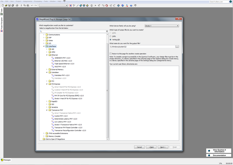
- First, open Quartus II, and create a new project with the New Project Wizard. Then open the MegaWizard Plugin manager, and select "Create a New Custom Megawizard Function." Select the PHY IP you want to generate (and choose the HDL you want to use and the directory for the resulting design files), using the Megawizard Plugin Manager and click "Next".
- See Figures 1-1, 1-2, and 1-3.
- Figure 1-1: Quartus MainScreen 5/52/Quartus_main_screen.png
- Figure 1-2: Megawizard Main Screen 3/3e/Megawizard_Main_Screen.png
- Figure 1-3: Choosing a PHY IP To Generate 7/79/Megawizard_Protocols.png
- Understand PHY IP Features and Customize the IP:
The MegaWizard will allow you to easily generate the Transceiver PHY IP, the Transceiver Reconfiguration Controller, and the Reset Controller. Refer to the V-Series Transceiver PHY IP Core User Guide, or Level 2 articles in the Transceiver Design Flow Series for more information about the IP.
- Generating PHY IP
A screen similar to Figure 3-1 will appear after completing step #1. Here you can edit parameters for the PHY IP to suit your design requirements. For details about the configurable settings for each PHY IP, see the V-Series Transceiver PHY IP Core User Guide "Parameter Settings" sub-section of each protocol section. When finished, click "Finish."
- Figure 3-1: PHY IP Configurable Parameter
- Quartus generates a <phy_ip_instance_name> folder, a <phy_ip_instance_name_sim> folder, <phy ip instance name>.qip, and a phy ip instance name.v. The folders contain lower-level design files used in compilation, and the phy_ip_instance_name.v is the top-level design file.

Repeat Steps 1-3 for the Reconfiguration Controller. You may also need to repeat Steps 1-3 for an external Reset Controller, depending on the Transceiver PHY IP you are implementing. For this article, we are implementing a Native PHY IP, which does require an external reset controller. To find out whether or not you need to instantiate your own Reset Controller, refer to the chapter that pertains to the Transceiver PHY IP you are implementing within the V-Series Transceiver PHY IP Core User Guide.
- Connect Transceiver PHY IP To Reconfiguration Controller
- In order to connect the Transceiver PHY IP to the Reconfiguration Controller, the user must implement the Reconfiguration Interface, which is coded according to the Avalon MM Specification.
- See chapter 12 of the V-Series Transceiver PHY IP Core User Guide for more information.
- Integrating the MegaWizard Generated IP Into the Overall Physical Layer Design
- The user generates only the Transceiver PHY IP, the Transceiver Reconfiguration controller, and the Reset Controller through the MegaWizard. It is up to the user to code the rest of the transceiver design by themselves.
- Compile the Design in ModelSim
- Writing a Compilation Script:
- You will need to create a .tcl script called phy_sim_top.tcl that contains compilation commands for: Stratix V Library files , Transceiver PHY IP Instance files , Reconfig Controller instance files , (Possibly Reset Controller Instance Files if the reset controller is external to the Transceiver PHY IP) , User created design files , the Top Level Testbench file , and Commands to invoke the simulator.
- make sure that the QUARTUS_ROOTDIR variable is set correctly in phy_sim_top.tcl. To be safe, use set QUARTUS_ROOTDIR <your_quartus_root_directory>.
- It is important that the compilation commands for MegaWizard generated files in the .Tcl be ordered as they are ordered in theplain_files.txtlocated within the _sim folder for each MegaWizard generated IP.
- You must also place all Altera generated IP into its own library (make a new library with the vlib <library_name>command).
- Use the phy_sim_top.tcl file located in the attached project as a reference.
- Once the phy_sim_top.tcl file has been generated, use the command source phy_sim_top.tcl within ModelSim to compile your design. After than use the command run -all to simulate an infinite amount of time. Use run <time> to simulate for a specific time.
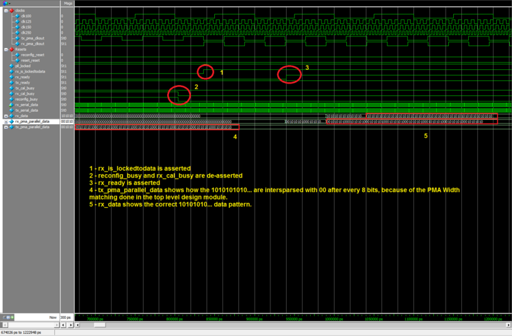
- Figure 6-1: Simulation Results (tx setup)
- Figure 6-2: Simulation Results (rx setup)
- Hardware Checkout
- When the design has been functionally verified in simulation, it is time to verify that the design works when ported to hardware. The pins must be connected using the Pin Planner, and assignments must be made using the Assignment Editor.
- Figure 7-1: Location of the Pin Planner and the Assignment Editor in the Quartus II GUI
- Figure 7-2: Pin Planner Assignments for the Reference Design
- Figure 7-3: Assignment Editor Screenshot for the Reference Design
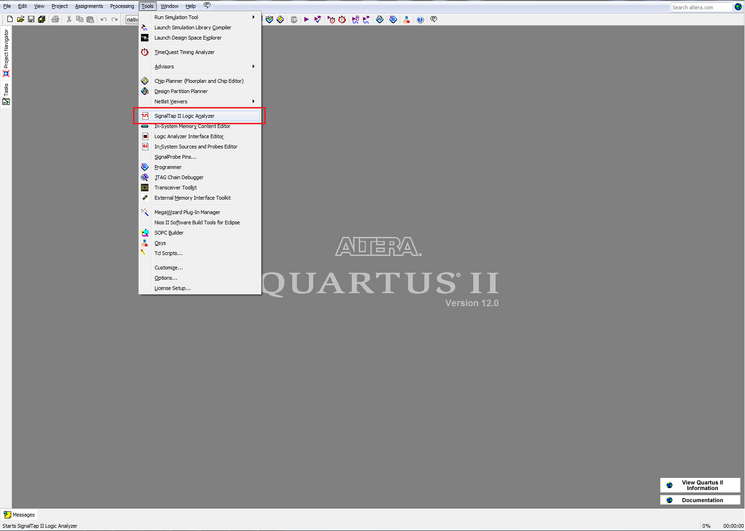
- Once these necessary assignments have been made, creating a signal tap file is time. Signal Tap is essentially an on-chip Logic Analyzer. The Logic Analyzer is coded into the FPGA fabric, which allows you to probe any signal within your design in real-time.
- Figure 7-4: Creating a Signal Tap File for the Project
- Figure 7-5: The Signal Tap GUI
- Create your .stp file using the GUI (steps 1-2 in Figure 7-5), then compile the design. Compilation should take about 30 minutes, depending on your machine. Afterward, program the device using the signal tap GUI (step 4 in Figure 7-5) and then run the logic analyzer (step 5 in Figure 7-5), switch to the data tab of the GUI to view your signals in real-time.
- This completes the walkthrough for the included reference design. Explore the Level 2 articles for more guides and technical information regarding Transceiver Design using Altera products.


Key Words
Stratix V, PCIE PIPE PHY IP, Tranceiver Reconfiguration Controller, Physical layer, PCI Express, Express, Stratix Five, GT, GS, GX, Design, Example, guide, walkthrough,
PCIe, PCI E, PCI Express, Stratix V, SV, S, V, Walkthrough, guide, help, Stratix V GX, Stratix V GT, SV, SVGX, SVGT, S5GX, S5GT, S5, Stratix 5, Stratix 5 GX, StratixV, StratixV GX, Stratix5, Stratix5 GX, Altera, generated, generation, Instantiation, creation, design, files,
© 2010 Altera Corporation. The material in this wiki page or document is provided AS-IS and is not
supported by Altera Corporation. Use the material in this document at your own risk; it might be, for example, objectionable,
misleading, or inaccurate.
Community support is provided Monday to Friday. Other contact methods are available here.
Intel does not verify all solutions, including but not limited to any file transfers that may appear in this community. Accordingly, Intel disclaims all express and implied warranties, including without limitation, the implied warranties of merchantability, fitness for a particular purpose, and non-infringement, as well as any warranty arising from course of performance, course of dealing, or usage in trade.
For more complete information about compiler optimizations, see our Optimization Notice.