Transceiver Reference Clock Phase Noise Jitter Calculator
Success! Subscription added.
Success! Subscription removed.
Sorry, you must verify to complete this action. Please click the verification link in your email. You may re-send via your profile.
- Intel Community
- Intel Community Knowledge Base
- Product Support Forums Knowledge Base
- FPGA Knowledge Base
- FPGA Wiki
- Transceiver Reference Clock Phase Noise Jitter Calculator
Transceiver Reference Clock Phase Noise Jitter Calculator
- Subscribe to RSS Feed
- Mark as New
- Mark as Read
- Bookmark
- Subscribe
- Printer Friendly Page
- Report Inappropriate Content
Transceiver Reference Clock Phase Noise Jitter Calculator
Last Major Update
Major Release - May 3rd 2012 - version 1.0 - added SV and ATX PLL support
Overview
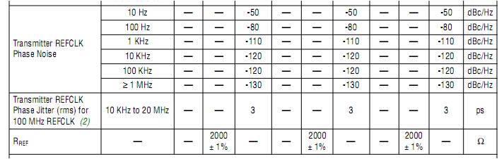
This article discusses a common issue of determining the phase noise jitter due to the reference clock in a typical transceiver application. Altera devices or transceivers usually specify the requirements of the reference clock in a table (see Figure 1) of offset frequency vs phase noise (dBc/Hz) however for many applications/protocols this specification is too general or too strict.
Figure 1: Example SIV REFCLK phase noise specification (from SIV Device Handbook, see latest Handbook for up to date specification)
0/0e/SIV_ref_clock_phase_noise_spec.jpg
To allow for a more accurate specification of reference clock phase noise, Altera has created a calculator tool where the user can enter their design configuration and estimate the impact the reference clock is having on the transmitter output jitter. Note that this is the primary purpose of this tool and the calculated jitter value is an ideal case approximation. Also be aware that this jitter is random jitter (RJ) only due to the phase noise from the reference clock and transmitter PLL, other factors in the system may effect this number.
To simplify the calculator and reduce the massive amount of data that would be required to accurately assess every PLL configuration, the calculator uses ideal jitter numbers to determine the worse case contribution from the reference clock. That is, when the PLL intrinsic phase noise is at its lowest, the reference clock’s phase noise will contribute a bigger percentage to the total. The calculator shows the PLL settings under which the ideal phase noise is determined. If the user is not using these settings then it can be assumed that the contribution to phase noise from the reference clock will be less than determined by the calculator as the PLL intrinsic phase noise will be higher
Please carefully note the assumptions and limitations listed below.
How to get the Reference Clock Phase Noise Jitter Calculator
The calculator is Matlab driven and requires the Matlab Compiler Runtime (MCR) engine v7.17. It can be installed without a license and can be downloaded from here:
www.mathworks.com/products/compiler/mcr/
The calculator executable is here:
64-bit version:
Altera_Reference_Clock_Phase_Noise_Jitter_Calculator.zip
32-bit version:
Altera_Reference_Clock_Phase_Noise_Jitter_Calculator_32bit.zip
Basic Analysis Theory
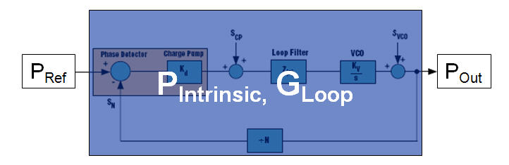
Total Jitter (TJ) on a transceiver output is made up of deterministic jitter (DJ) summed with random jitter (RJ). One source of RJ is from the phase noise of the reference clock and the Tx channel's PLL. See figure 2 for a simple diagram.
Figure 2: Basic PLL diagram d/dd/Phase_noise_in_PLL.jpg
The phase noise output of the PLL can be approximated as Pout = Pin + Pdiv + Pcp + Pvco +Plf where Pin is the input phase noise from the reference multiplied by the closed loop gain function (Gloop). Other components are the effects of the PLL sub blocks. We can sum these sub blocks into one number call Pintrinsic so:
Pout = Pref x Gloop + Pintrinsic
The output phase noise can be converted into phase jitter by integrating the area under the phase noise curve for each data point and taking the sum of root squares providing a psec (rms) value.
Calculator User Guide
Installation:
No installation is required to run the calculator itself, however the calculator requires the Matlab Compiler Runtime engine (v7.17) be installed (see above)
Getting Started:
Double click the .exe, the calculator may take a minute or so to load as the Matlab Compiler Runtime engine will first launch in the background.
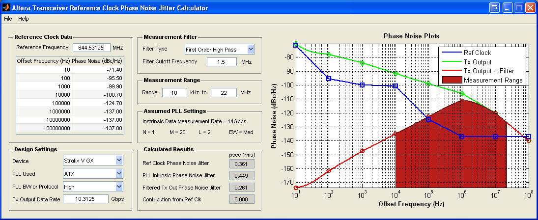
The calculator GUI looks similar to this: a/a4/Ref_Clock_Jitter_Calculator_GUI_Image.jpg
The entry fields are as follows:
- Reference Frequency - enter the frequency of the reference clock in MHz
- Reference Clock Phase Noise data table - enter the data points for the particular reference clock source of interest
- Device - enter Altera device family
- PLL Used - enter type of PLL used
- PLL BW or Protocol - either enter PLL BW (from Quartus) or protocol used
- Tx Output Data Rate - enter the data rate of the transceiver link in Mbps
- Measurement Filter Type - pick the measurement filter shape or No Filter if not required
- Measurement Filter Cutoff Frequency - enter the cutoff frequency of the measurement filter (if applicable)
- Measurement Range - enter the start and end frequency over which the jitter will be calculated, this is usually specified by the protocol
The calculator will automatically update the results each time a value is changed.
Usage Notes:
- The phase noise data must be listed in ascending order, leave the lower rows empty if not enough data is available
- When entering the phase noise data for the reference clock ignore spurious response frequencies that maybe seen in the offset phase noise measurement (ie. large spikes coming up from the phase noise curve). These spurs contribute to deterministic jitter, not random jitter
- The PLL BW/Protocol box sets the parameters for the PLL loop filter used in the analysis. Potentially there may be no observable changes to the phase noise results. This is because the loop filter only acts on the reference clock phase noise and not the PLL intrinsic phase noise which in most systems dominants the analysis
- The measurement filter is specified by some protocols when measuring jitter on a transmitter output to take into account the tracking abilities of the receiver CDR. The brickwall filter assumes -40dB of attenuation in the stopband
- The measurement range must be within the phase noise data points provided
- The Assumed PLL Settings box, shows the configuration of the selected PLL that the intrinsic phase noise is determined from. If the user is not using this configuration it can be assumed that the intrinsic phase noise will be similar or worse and thus the impact from the reference clock phase noise on output jitter will actually be less than reported. In most cases the difference will be negligible.
Saving Settings:
The calculator will automatically save the current settings when exiting and reload these when the calculator is started next. Users can also save and load data sets to .mat files under the File menu.
Results Analysis:
The tool calculates four phase noise jitter values in the system, all measured as psec (rms):
- Reference clock phase noise jitter - this is the jitter calculated directly from the phase noise data points entered in the table across the measurement range
- PLL intrinsic phase noise jitter - jitter from the PLL itself
- Tx out + filter phase noise jitter - jitter on the Tx port after the measurement filter is applied
- Contribution from the reference clock - this is the psec (rms) that the reference clock contributes to the Tx out + filter phase noise jitter number. It is determined by setting the reference clock phase noise to the noise floor and passing this data through the analysis and subtracting this figure from the measurement in (3)
The calculator does not determine if the jitter estimated on the Tx output is good or bad. This is up to the user depending on their system link, protocol specification or other requirements etc. It's important to note that some protocols like PCIe set specifications of random jitter for the reference clock itself, as well as the Tx out. In these protocols, to meet compliance the reference clock should meet the required spec, the calculator could be used to determine the random jitter if only the phase noise information is available for the reference clock.
The plot window shows the phase noise vs offset frequency at various points in the analysis.
For a typical xtal oscillator reference clock users will notice that it's phase noise has minimal effect on the Tx output jitter. This is expected for several reasons:
- The PLL loop filter will remove the high frequency phase noise from the reference clock
- The PLL intrinsic phase noise should be larger than the reference clock phase noise and thus dominant on the Tx output
- In some protocols a high pass filter is placed on the Tx output when measuring jitter. This is to account for the low frequency tracking ability of the Rx CDR and thus the noise at these frequencies are removed from the calculation.
The passband between the PLL's low pass filter cutoff and the CDR's high pass filter cutoff is in the approximate range between 1 to 10MHz. Thus if the reference clock does have poor phase noise performance only this range should really matter and then only if the phase noise is around or above the level of the PLL intrinsic noise.
Calculator Assumptions and Limitations
Currently the calculator tool only supports:
- Stratix IV and Stratix V
- Use Stratix V numbers for an approximation for Arria V until further notice
Assumptions:
- The calculator only estimates random jitter (RJ) on the Tx out port of a transceiver due to the reference clock and CMU PLL phase noise
- Other jitter sources like power supplies etc are not modeled. This calculator is just assessing the impact of the reference clock phase noise against the PLL's contribution
- Deterministic jitter (DJ) due to the reference clock is not analyzed. This is usually due to the DCD spec of the clock and in typical clock sources it should be small
Known Issues
- The ref clock phase noise entry table may have some viewing issues in Windows 7, it doesnt affect the functionality of the tool
Update History
- Initial Release - June 8th 2011 - version 0.2 BETA
- Major Release - May 3rd 2012 - version 1.0 - added SV and ATX PLL support
Key Words
Transceivers, Reference Clock, Random Jitter, Phase Noise Jitter, CMU ATX PLL
© 2010 Altera Corporation. The material in this wiki page or document is provided AS-IS and is not
supported by Altera Corporation. Use the material in this document at your own risk; it might be, for example, objectionable,
misleading or inaccurate. Retrieved from http://www.alterawiki.com/wiki/Altera_Wiki
|
|
Community support is provided Monday to Friday. Other contact methods are available here.
Intel does not verify all solutions, including but not limited to any file transfers that may appear in this community. Accordingly, Intel disclaims all express and implied warranties, including without limitation, the implied warranties of merchantability, fitness for a particular purpose, and non-infringement, as well as any warranty arising from course of performance, course of dealing, or usage in trade.
For more complete information about compiler optimizations, see our Optimization Notice.