- 新着としてマーク
- ブックマーク
- 購読
- ミュート
- RSS フィードを購読する
- ハイライト
- 印刷
- 不適切なコンテンツを報告
I'm trying to create a simple circuit, using 4 switches (8-4-2-1) to drive digital logic, in order to light a single 7-segment LED.
I've created the 4 input pins, wired them to inputs A,B,C, and D of a 7447 (BCD to 7-segment decoder), and wired the 7 outputs OA through OG) to output pins. I've tied the other 3 inputs (LTN, RBIN, BIN) to ground. I've assigned switches 0 through 3 to the inputs, and HEX0[*] to the outputs. However, when I compile, I get warnings that: Warning: Design contains 4 input pin(s) that do not drive logic Warning (15610): No output dependent on input pin "B" Warning (15610): No output dependent on input pin "C" Warning (15610): No output dependent on input pin "D" Warning (15610): No output dependent on input pin "A" Warning: Following 7 pins have nothing, GND, or VCC driving datain port -- changes to this connectivity may change fitting results Info: Pin OA has VCC driving its datain port Info: Pin OB has VCC driving its datain port Info: Pin OC has VCC driving its datain port Info: Pin OD has VCC driving its datain port Info: Pin OE has VCC driving its datain port Info: Pin OF has VCC driving its datain port Info: Pin OG has VCC driving its datain port Downloading to the DE2 board yields no results. The HEX0 (rightmost) 7 segment display is off, and no change in the input switches produces any change. It seems that the 7447 chip is not being utilized correctly... That the input pins are not connected to inputs on the 7447, and likewise for the outputs. I don't think I'm doing anything wrong with wiring or pin assignments; when I connect a switch directly to an LED, it works fine. If I put an inverter between them, that works fine. But the 7447 doesn't seem to work correctly. Any suggestions?コピーされたリンク
4 返答(返信)
- 新着としてマーク
- ブックマーク
- 購読
- ミュート
- RSS フィードを購読する
- ハイライト
- 印刷
- 不適切なコンテンツを報告
Maybe could be usefull if you post some of the code that you've done, to help you.
- 新着としてマーク
- ブックマーク
- 購読
- ミュート
- RSS フィードを購読する
- ハイライト
- 印刷
- 不適切なコンテンツを報告
As I said, I did the design via schematic. Here is a screenshot:
http://farm4.static.flickr.com/3236/2887864395_823e7d95da.jpg The circuit on the top is what I'm trying to get working; the switch-inverter-LED on the bottom was just to verify that I hadn't missed something on the real circuit.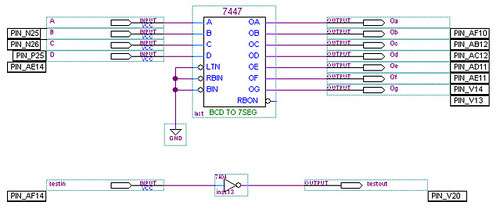
- 新着としてマーク
- ブックマーク
- 購読
- ミュート
- RSS フィードを購読する
- ハイライト
- 印刷
- 不適切なコンテンツを報告
Try this:
LTN = H RBIN = X BIN = H You've this: LTN = L RBIN = L BIN = L Then ignore the warnings.- 新着としてマーク
- ブックマーク
- 購読
- ミュート
- RSS フィードを購読する
- ハイライト
- 印刷
- 不適切なコンテンツを報告
That should do it, thanks. All the warnings threw me for a loop, when I should have been looking at the data sheet more closely.