- Отметить как новое
- Закладка
- Подписаться
- Отключить
- Подписка на RSS-канал
- Выделить
- Печать
- Сообщить о недопустимом содержимом
Hi
I'm building 2d fft for image processing from the design example provided by Altera, namely modify it to take advantage of Hermitian symmetric: use N/2 point fft to perform a N point real-to-complex fft transform. One problem that bothered me a while is that though it only need to do N/2 point fft, it actually produce N/2+1 output and that +1 is necessary for inverse transform, so in the transpose kernel I have to somehow output one more data each row (or 8 data each working-group) and that extra output will mess the whole performance up. The kernel originally was writing 8 float2 (that is 512 bits) to global memory, and I added more 8 float2 sets writing under different branches and it works fine, what really changes the structure is when I want to write more then 8 float2 (either to the same cl_buffer or different buffer), the store unit will be construct with different width and much more latency, 72 instead of 2 in my case, as you can see in the picture. dest.x = buf.x*A - buf.y*A + buf.x*B + buf.y*B; dest.y = buf.y*A + buf.x*A + buf.x*B - buf.y*B;
dest.x = buf.x*A - buf.y*A + buf.x*B + buf.y*B;
dest.y = buf.y*A + buf.x*A + buf.x*B - buf.y*B;
dest.x = buf.x*A - buf.y*A + buf.x*B + buf.y*B;
dest.y = buf.y*A + buf.x*A + buf.x*B - buf.y*B;
dest.x = buf.x*A - buf.y*A + buf.x*B + buf.y*B;
dest.y = buf.y*A + buf.x*A + buf.x*B - buf.y*B;
dest.x = buf.x*A - buf.y*A + buf.x*B + buf.y*B;
dest.y = buf.y*A + buf.x*A + buf.x*B - buf.y*B;
dest.x = buf.x*A - buf.y*A + buf.x*B + buf.y*B;
dest.y = buf.y*A + buf.x*A + buf.x*B - buf.y*B;
dest.x = buf.x*A - buf.y*A + buf.x*B + buf.y*B;
dest.y = buf.y*A + buf.x*A + buf.x*B - buf.y*B;
dest.x = buf.x*A - buf.y*A + buf.x*B + buf.y*B;
dest.y = buf.y*A + buf.x*A + buf.x*B - buf.y*B;
//dest2.x= buf.x - buf.y;//this two lines make all the difference
//dest2.y = 0;
// or this one:
//dest.x = buf.x*A - buf.y*A + buf.x*B + buf.y*B;
https://alteraforum.com/forum/attachment.php?attachmentid=14454&stc=1 https://alteraforum.com/forum/attachment.php?attachmentid=14455&stc=1 Eventually I worked around it by using channels to passed the extra data to a new kernel and let it write to global memory. I can't find anything about this 512 width global memory access constrain or optimization in the documents, anyone know why the compiler is building the store units this way? Thanks.
Ссылка скопирована
- Отметить как новое
- Закладка
- Подписаться
- Отключить
- Подписка на RSS-канал
- Выделить
- Печать
- Сообщить о недопустимом содержимом
Images attached to posts in the forum seem to be automatically shrinked and compressed; it is impossible to see anything in your image. Can you post it somewhere else? Or better yet, attach the complete "report" folder?
Furthermore, I am not sure if I understand what your problem is; are you wondering why load/store units which are larger than 512 bits incur higher latency?- Отметить как новое
- Закладка
- Подписаться
- Отключить
- Подписка на RSS-канал
- Выделить
- Печать
- Сообщить о недопустимом содержимом
Hi HRZ
I made the picture larger. It's not all case that write to global with more than 512 bits will this situation occur, e.g. without the if else branch. You can try to compile the code below and see the difference in the system viewer when line in question is marked out. Thank you.__kernel void test(global float2 *restrict dest, global float2
*restrict in, int i)
{
local float2 buf;
int where = get_local_id(0);
int N=64;
buf = in;
buf = in;
buf = in;
buf = in;
buf = in;
buf = in;
buf = in;
buf = in;
if (i){
dest = buf;
dest = buf;
dest = buf;
dest = buf;
dest = buf;
dest = buf;
dest = buf;
dest = buf;
dest = buf; // this line
}
else {
dest = buf;
dest = buf;
dest = buf;
dest = buf;
dest = buf;
dest = buf;
dest = buf;
dest = buf;
}
}
- Отметить как новое
- Закладка
- Подписаться
- Отключить
- Подписка на RSS-канал
- Выделить
- Печать
- Сообщить о недопустимом содержимом
I don't see anything out of the ordinary in the report from your sample code. The compiler creates a 512-bit coalesced load from global memory, and two stores, one of of which is 512 bits wide and the other is 64 bits; since the size of global memory ports must be a power of two, the compiler is deciding that it is best if your 9 consecutive stores are split into one big and one small store, instead of a bigger 1024-bit store (which will waste a lot of memory bandwidth). This decision seems correct to me. Furthermore, the compiler is combining your stores from the if and the else, since the write addresses are the same and only the data is different; hence, the compiler can just instantiate a multiplexer to send the correct data to memory, instead of creating extra memory ports.
Regarding latency, I am not seeing any specific difference. You are not comparing the latency from the "white" store unit which belong to your local buffer, with the "blue" store units from the global buffer, are you? Finally, you should note that the actual latency of accesses to/from global memory is over 100 cycles; the latency the compiler reports for these accesses only depends on the number of extra registers the compiler inserts on the way to the memory port to absorb stalls, and does not reflect the real latency of the accesses. If the accesses finishes in less clocks than there are registers on its way, the pipeline will not be stalled (but some bubbles might be inserted). However, if the access takes longer, then the pipeline will stall. At the end of the day, having more registers on the way of global memory accesses will be beneficial since it allows absorbing more stalls, but will come at the cost of higher area usage.- Отметить как новое
- Закладка
- Подписаться
- Отключить
- Подписка на RSS-канал
- Выделить
- Печать
- Сообщить о недопустимом содержимом
Hi HRZ
Thank you for the reply. I'm compiling for Arria 10 and I did see significant different (2 vs 50+2 as marked in the picture), and it did reflect latency when running on FPGA (512*512 2d FFT 0.8ms vs 2.5ms). https://imgur.com/a/7eqlr It's what the compiler think is best for you but in actual practice it's not optimal and programmer have to deal with it...:o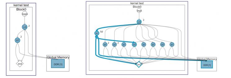
- Отметить как новое
- Закладка
- Подписаться
- Отключить
- Подписка на RSS-канал
- Выделить
- Печать
- Сообщить о недопустимом содержимом
The new image you have posted looks completely different from what I got from compiling your original kernel. In the new case, the reason for the slow-down is not the difference in latency, but rather the fact that now, instead of one read and one write port going to external memory, you have one read and 9 writes, all of which will be competing with each other to obtain access to the memory bus. This will result in a very high amount of contention and very frequent stalls in memory accesses which will get propagated all the way down to the pipeline. If this is one of those cases that the compiler is failing to coalesce the accesses, even though they are consecutive, then, yes, the compiler is making a mistake here (I reported one such case to Altera long ago). If not, you should modify your kernel to minimize the number of write ports.
Unless your input is so small that the pipeline is not filled before execution finishes, the "latency" of the pipeline will not have a noticeable effect on run time.- Отметить как новое
- Закладка
- Подписаться
- Отключить
- Подписка на RSS-канал
- Выделить
- Печать
- Сообщить о недопустимом содержимом
I did more tests, you are right about the compiler combining the stores in the if/else branches, that's why it have two layers and cascading write units have large latency.
If both branches have 9 writes it's would use one 1024bits write, thought more bandwidth usage but the latency is small and that's what I care about. But in my case the 9th write in the else branch is a "void write" and may cause wrong output if kernel execution ordering is not sequential (not sure if it is, I think I read it somewhere that it's not guaranteed, but it is sequential in my experience) I wish programmer could just specify "don't try to share write unit between branches" or "use largest bandwidth necessary in any one branch"- Отметить как новое
- Закладка
- Подписаться
- Отключить
- Подписка на RSS-канал
- Выделить
- Печать
- Сообщить о недопустимом содержимом
Having one write per branch will most likely give you even lower performance due to even more contention on the memory bus. Remember that with the kernel running at the same operating frequency as the memory controller (266 MHz in case of 2133 MHz memory) the FPGA external memory bandwidth will be saturated with two 512-bit accesses (read or write) per clock. If you have two 1024-bit accesses just for writing, and also some reads, then you are going to get a huge amount of contention on the memory bus.
In NDRange kernels, sequentially of threads is not guaranteed, but sentimentality of operations per thread is guaranteed.- Отметить как новое
- Закладка
- Подписаться
- Отключить
- Подписка на RSS-канал
- Выделить
- Печать
- Сообщить о недопустимом содержимом
--- Quote Start --- Remember that with the kernel running at the same operating frequency as the memory controller (266 MHz in case of 2133 MHz memory) the FPGA external memory bandwidth will be saturated with two 512-bit accesses (read or write) per clock. --- Quote End --- Thank you for the information, I'm not aware of this. Why would kernel running at 266MHz with 2133MHz memory saturate at 1024bits access? Any documentation? Thanks.
- Отметить как новое
- Закладка
- Подписаться
- Отключить
- Подписка на RSS-канал
- Выделить
- Печать
- Сообщить о недопустимом содержимом
There is no documentation on this, but this can be calculated by taking the kernel and memory operating frequency and the width of the memory bus into account.
The bus width per bank for DDR3 and DDR4 memory is 64 bits (72 bits with ECC). The memory operating frequency for DDR3 is generally 1600 MHz (800 MHz double data-rate), and for DDR4 is 2133 MHz (1066 MHz double data-rate). The memory controller on the FPGA runs at 1/8 of the clock of the external memory for these two memory types. Hence, the memory bandwidth will be saturated if the kernel is running at the same operating frequency as the memory controller, but the accesses are at least 8 times larger than the width of the memory bus. To this end, for 2 banks of DDR4 memory running at 2133 MHz, a kernel running at 266 MHz with a total access size of bus_width x number_of_banks x (memory_frequency/kernel_frequency) = 64 x 2 x 8 = 1024 bits per clock will saturate the memory bandwidth. Of course this will only happen in a 100% ideal scenario: - Your kernel has only one read and one write, both of which are 512 bits wide - The number of reads and writes are the same - The read and write buffers are manually partitioned into the two banks - Memory accesses are all aligned - The kernel is running exactly at 266 MHz - There is no other source of stalling in your kernel (e.g. channels) In practice, you might still get marginal performance improvement with a total access size of larger than 1024 bits per clock, since the memory controller is far from perfect, but if you have multiple access ports to memory, performance is more likely to go down with larger accesses, rather than up. At the end of the day, you should try to minimize the number of access ports to external memory, but maximize the size of the accesses.- Отметить как новое
- Закладка
- Подписаться
- Отключить
- Подписка на RSS-канал
- Выделить
- Печать
- Сообщить о недопустимом содержимом
Thanks a lot, that's really helpful for understanding the architecture. :)
- Подписка на RSS-канал
- Отметить тему как новую
- Отметить тему как прочитанную
- Выполнить отслеживание данной Тема для текущего пользователя
- Закладка
- Подписаться
- Страница в формате печати