- Mark as New
- Bookmark
- Subscribe
- Mute
- Subscribe to RSS Feed
- Permalink
- Report Inappropriate Content
From some example, I know some meaning of suffix by my guessing.
Ex.
"clk" is the clock pin of a D flip-flop.
"q" is the output pin of a D flip-flop.
"~0" to "~*" are the duplicate nets. Note that * represent any number.
"~clkctrl" is the global buffer by my guessing.
Does there have a complete table to describe all the suffix meaning?
Thank you very much.
Link Copied
- Mark as New
- Bookmark
- Subscribe
- Mute
- Subscribe to RSS Feed
- Permalink
- Report Inappropriate Content
What are you referring to? Are you talking about selecting items in a timing netlist for creating timing constraints? Where are you looking at this and what's your goal?
- Mark as New
- Bookmark
- Subscribe
- Mute
- Subscribe to RSS Feed
- Permalink
- Report Inappropriate Content
Hi sstrell
I want to know the the suffix meaning.
For example, the "_clk" is the clock pin of a D flip-flop. "A_clk" is D flip-flop A's clock pin.
Does there have some document for reference? Thank you very much.
- Mark as New
- Bookmark
- Subscribe
- Mute
- Subscribe to RSS Feed
- Permalink
- Report Inappropriate Content
Hello,
Yes, could you share first which document are you referring to?
Regards,
Aqid Ayman
- Mark as New
- Bookmark
- Subscribe
- Mute
- Subscribe to RSS Feed
- Permalink
- Report Inappropriate Content
Hi AqidAyman_Intel
I don't know which document I can refer.
For example, I know inclk[*] is the generated clock pin of PLL from "drive_pll_clocks" command.
I know that the "_clk" is the clock pin of a D flip-flop from some SDC constraint example.
I want to know the the suffix meaning.
Does there have some document for reference? Thank you very much.
- Mark as New
- Bookmark
- Subscribe
- Mute
- Subscribe to RSS Feed
- Permalink
- Report Inappropriate Content
I'm still not sure what you are looking for. It does seem, though, you are referring to the timing netlist when performing a timing analysis. You can right-click anything and cross-probe to other tools by selecting one of the Locate options. For example, you could cross probe from a timing analyzer report to the RTL Viewer or Technology Map Viewer to see pins on an entity, like a PLL.
- Mark as New
- Bookmark
- Subscribe
- Mute
- Subscribe to RSS Feed
- Permalink
- Report Inappropriate Content
Hi sstrell
Yes, like that.
But I don't want to open RTL Viewer or Technology Map Viewer every time.
Like the Design Compile tool on SoC synthesis flow, all register names are named "****_reg".
All output pin of a register is named "****_reg.Q".
All clock pin of a register is named "****_reg.CLK".
The duplicated register's output is named "****_reg~0.Q".
The bit 1 of a register is named "****_reg_1.Q".
It is a naming rule that defined by the tool.
I need it to help people to quickly find the node that they want to.
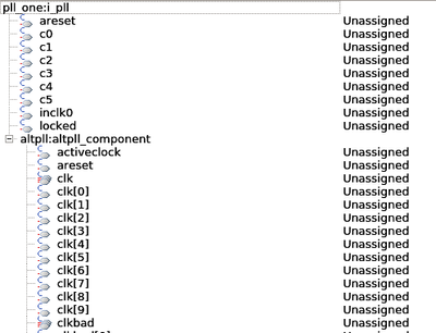
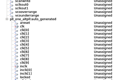
Back to the PLL on FPGA, there are many pins in PLL module, like follows picture.
I don't know which pin I should constraint.
I don't know which pin I can constraint.
I only know which pin should be constrained the clock constraint from the "drive_pll_clocks" command.
Thank you very much.
- Mark as New
- Bookmark
- Subscribe
- Mute
- Subscribe to RSS Feed
- Permalink
- Report Inappropriate Content
I think you're overthinking this a bit. If your goal is to fully constrain your design for timing, all you need (at a minimum) are clock constraints and I/O constraints. Timing exceptions are optional, though usually required.
For a PLL, the command is derive_pll_clocks (not "drive_pll_clocks") and that command alone defines the output clock domains of the PLL, targeting the output pins of the PLL. They're c0 through c5 in the screenshot you've posted, but the nice thing about the tool and the command is that you don't need to know that to constrain the design. If you add the -create_base_clocks option, that constrains the reference clock into the PLL (inclk0). And with that, you're done (for the clocks that is).
If you are missing constraints, rely on the Unconstrained Paths report from the timing analyzer to find the paths the tool considers to be unconstrained and then constrain them. This report lists unconstrained clock and I/O paths.
- Mark as New
- Bookmark
- Subscribe
- Mute
- Subscribe to RSS Feed
- Permalink
- Report Inappropriate Content
Hi sstrell
Thank you, sstrell, very much. I have two questions more.
1. If I use an exception timing constraint on/for a pre-synthesis node, does it work after post-fitter?
Some nodes may is disappeared after post-fitter.
In SoC follow, user always uses the node name which comes from after synthesis.
But I don't know the node name which comes from after post-fitter that can be used for SDC.
2. When I report timing path report, how can directly know the the node name which comes from after post-fitter?
For example, I know the combination output name after post-fitter called "*|combout". So, I can report the specified path delay.
If I don't know that, how can I to directly report the specified path delay?
Thank you very much.
- Mark as New
- Bookmark
- Subscribe
- Mute
- Subscribe to RSS Feed
- Permalink
- Report Inappropriate Content
1) Timing exceptions don't typically affect whether logic is optimized away during compilation. I can't think of a situation where this would be applicable. In fact, timing exceptions usually prevent logic from being optimized away and prevent optimization in some devices (like Stratix 10 and Agilex Hyperflex devices).
2) In the graphical Timing Analyzer tool, you can use the Node Finder in most dialog boxes when you create custom timing reports. The Name Finder lets you search the timing netlist for the resource or path in question similar to using the Node Finder to target nodes or entities for assignments or use in other tools. You set the Name Finder filter to the get_pins collection to find specific pins on a cell (like combout).
- Mark as New
- Bookmark
- Subscribe
- Mute
- Subscribe to RSS Feed
- Permalink
- Report Inappropriate Content
Hi sstrell
Thank you, sstrell, very much. I get it. But.....
Unfortunately, all beginners don't know what is the mean of "combout" when use get_pins in Node Finder.
What can I do for that?
For me, I guess "combout" is the output of a cell. And then I search some information to confirm it on the Google.
If I can't find any information on the Google, what is the next step?
Thank you very much.
- Mark as New
- Bookmark
- Subscribe
- Mute
- Subscribe to RSS Feed
- Permalink
- Report Inappropriate Content
"combout" means "combinational logic output". These are basic digital logic design shorthand names. It's expected that if you are doing digital logic design that you are familiar with things like this. I think this is the type of stuff you learn in college or university and is a given if you are doing this type of design.
- Mark as New
- Bookmark
- Subscribe
- Mute
- Subscribe to RSS Feed
- Permalink
- Report Inappropriate Content
Hi sstrell
Thank you, sstrell, very much.
Can I know what kind of situation that the output name is named "combout"?
From the logic cell document, I know data{a~f} is the input pin of logic cell of FPGA.
How about "combout"?
Thank you very much.
- Mark as New
- Bookmark
- Subscribe
- Mute
- Subscribe to RSS Feed
- Permalink
- Report Inappropriate Content
I just said that combout is a digital logic output. In the case of the FPGA, this would be the output of a lookup table (LUT) or logic element (LE).
- Mark as New
- Bookmark
- Subscribe
- Mute
- Subscribe to RSS Feed
- Permalink
- Report Inappropriate Content
Hi sstrell
Thank you, sstrell, very much. I get it.
Does there have document to tell the user how Quartus change the name between RTL and fitter?
Thank you very much.
- Mark as New
- Bookmark
- Subscribe
- Mute
- Subscribe to RSS Feed
- Permalink
- Report Inappropriate Content
Hello,
What do you mean by Quartus change the name between RTL and fitter? Can you clarify?
- Subscribe to RSS Feed
- Mark Topic as New
- Mark Topic as Read
- Float this Topic for Current User
- Bookmark
- Subscribe
- Printer Friendly Page


