- Mark as New
- Bookmark
- Subscribe
- Mute
- Subscribe to RSS Feed
- Permalink
- Report Inappropriate Content
Hi all,
I was trying to write a verilog code for a memory module which has has a bidirectional inout port for the data. But I also want to output high impedance during write or if MEM_OE(output enable) is not set. But my code as below cannot simulate the reading correctly... It outputs high impedance even after I enabled the MEM_OE and do the reading. Plz help me, thanks in advance!
module memory_emb(address, MEM_RW, MEM_OE, MEM_DATA, clk);
input  address;
input MEM_RW, MEM_OE;
//MEM_OE=1 for memory output enable, MEM_OE=0 output=ZZZZ...
//MEM_RW=0 for read, MEM_RW=1 for write
inout  MEM_DATA;
input clk;
wire  MEM_DATA;
reg  data_out; //internal wire
reg  Memory ;
assign MEM_DATA=(MEM_OE&&!MEM_RW)?data_out:18'bz;
always@(posedge clk)
begin
  if(!MEM_RW&&MEM_OE)
    data_out<=Memory;
  else if(MEM_RW&&MEM_OE)
    begin
      Memory<=MEM_DATA;

    end
end
endmodule
Link Copied
17 Replies
- Mark as New
- Bookmark
- Subscribe
- Mute
- Subscribe to RSS Feed
- Permalink
- Report Inappropriate Content
And there was a warning for this code after i did the compilation
Warning: Inferred dual-clock RAM node "Memory~0" from synchronous design logic. The read-during-write behavior of a dual-clock RAM is undefined and may not match the behavior of the original design. Will this be where the problem comes from? How could I edit my code to avoid that?- Mark as New
- Bookmark
- Subscribe
- Mute
- Subscribe to RSS Feed
- Permalink
- Report Inappropriate Content
Don't use this assignment in the always process
Memory[address]<=MEM_DATA; Try instead this: Memory[address]<=data_in; Where: wire [17:0] data_in; assign data_in = MEM_DATA;- Mark as New
- Bookmark
- Subscribe
- Mute
- Subscribe to RSS Feed
- Permalink
- Report Inappropriate Content
anyway your code works in Quartus simulator.
check out: you declared 12-bit wide address bus, but just 256 memory cell. maybe error in simulation? and pay attention that reading process is not just one clock like writing.- Mark as New
- Bookmark
- Subscribe
- Mute
- Subscribe to RSS Feed
- Permalink
- Report Inappropriate Content
Hi bark,
Yea, I got errors in simulation. And I know if I call a memory megafunction from Altera, the module for reading and writing could take more than 1 cyle to do them. But what if I only need to synthesize a code which can do read in one cycle and do write in one cycle?- Mark as New
- Bookmark
- Subscribe
- Mute
- Subscribe to RSS Feed
- Permalink
- Report Inappropriate Content
Cris72,
Thank you. But the problem is still not solved. I still cannot ouput real values other than ZZZZ when after read.- Mark as New
- Bookmark
- Subscribe
- Mute
- Subscribe to RSS Feed
- Permalink
- Report Inappropriate Content
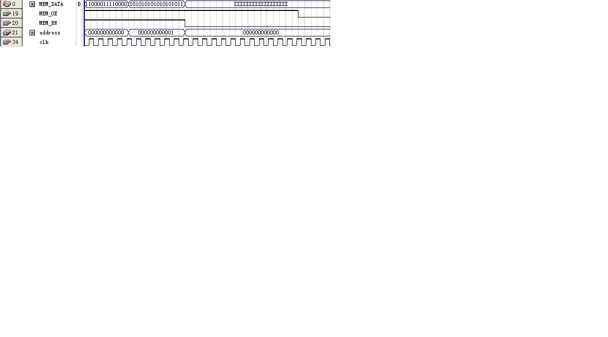
I just posted the simulation result in the attachment.
- Mark as New
- Bookmark
- Subscribe
- Mute
- Subscribe to RSS Feed
- Permalink
- Report Inappropriate Content
- Mark as New
- Bookmark
- Subscribe
- Mute
- Subscribe to RSS Feed
- Permalink
- Report Inappropriate Content
bark,
Oh so the read operation has to take two cycles if i want to use memory... Then how should i modify my verilog code?- Mark as New
- Bookmark
- Subscribe
- Mute
- Subscribe to RSS Feed
- Permalink
- Report Inappropriate Content
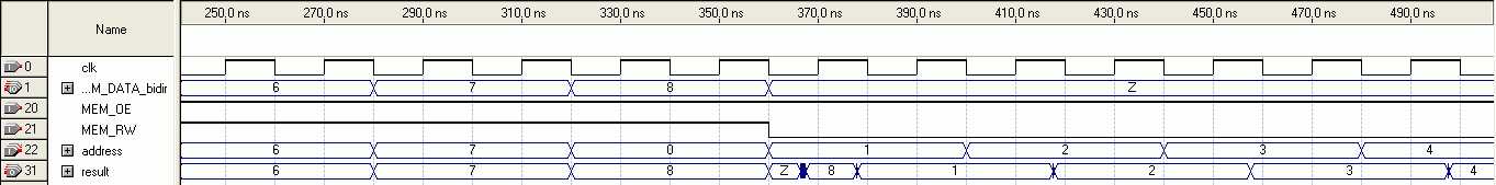
bark,
how did you get the simulation right? I cannot find the O MEM_Data_Bidir value in the simulation list...- Mark as New
- Bookmark
- Subscribe
- Mute
- Subscribe to RSS Feed
- Permalink
- Report Inappropriate Content
I just renamed MEM_Data to MEM_Data_Bidir.
I did nothing with sources. Only compile it in QuartusII9.1 and simulate. If you remove data_out register and make output like this: assign MEM_DATA_bidir = Read ? Memory[address] : 'z ; then compilator will not optimise regs to memory. But anyway I didn't get one clock read operation.- Mark as New
- Bookmark
- Subscribe
- Mute
- Subscribe to RSS Feed
- Permalink
- Report Inappropriate Content
my current src:
module mem_test(address, MEM_RW, MEM_OE, MEM_DATA_bidir, clk); input [7:0] address; input MEM_RW, MEM_OE; //mem_oe=1 for memory output enable, mem_oe=0 output=zzzz... //mem_rw=0 for read, mem_rw=1 for write inout [17:0] MEM_DATA_bidir; input clk; reg [17:0] data_out; wire [17:0] MEM_DATA; reg [17:0] Memory [0:255]; wire Read = MEM_OE && (!MEM_RW) ; wire Write = MEM_OE && MEM_RW ; assign MEM_DATA_bidir = Read ? data_out : 'z ; always@(posedge clk) begin if (Write) Memory[address] <= MEM_DATA_bidir ; data_out <= Memory[address] ; end endmodule- Mark as New
- Bookmark
- Subscribe
- Mute
- Subscribe to RSS Feed
- Permalink
- Report Inappropriate Content
--- Quote Start --- But anyway I didn't get one clock read operation. --- Quote End --- I don't exactly understand what's going on in your simulation. A RAM with unregistered outputs will send the data after latching the read address, without an additional cycle of delay. You can check in the respective device handbooks. Also your Verilog code is specifying this operation. So the design compiler should either implement or reject it, but not add a delay cycle. Did you perform a functional or timing simulation? What's the involved device, what's the clock frequency?
- Mark as New
- Bookmark
- Subscribe
- Mute
- Subscribe to RSS Feed
- Permalink
- Report Inappropriate Content
CycloneIII C7 100Mhz
one clock operation in case if all memory compile in logic registers. not memory. my simulation on previous page was for memory. and seems to be working fine. outputs in simulation was not VirtualPins. it cost + several ns to timings I hope I am expressing myself correctly =)- Mark as New
- Bookmark
- Subscribe
- Mute
- Subscribe to RSS Feed
- Permalink
- Report Inappropriate Content
- Mark as New
- Bookmark
- Subscribe
- Mute
- Subscribe to RSS Feed
- Permalink
- Report Inappropriate Content
Thanks you guys. Now I have figured out what's wrong with my original code.
In my original code below, i shouldn't have included MEM_OE condition in the always block. That should only appear with the assign statement. That's kind of a standard way of manipulating this bi-directional port stuff. In this case, the MEM_RW actually represents the select signal for tri-state buffer in the bi-directional port.
assign MEM_DATA=(MEM_OE&&!MEM_RW)?data_out:18'bz;
always@(posedge clk)
begin
  if(!MEM_RW&&MEM_OE)
    data_out<=Memory;
  else if(MEM_RW&&MEM_OE)
    begin
      Memory<=MEM_DATA;

    end
end
- Mark as New
- Bookmark
- Subscribe
- Mute
- Subscribe to RSS Feed
- Permalink
- Report Inappropriate Content
you don't need if for data_out assign.
for example in recommended hdl coding styles memory written that: begin if (we) mem[write_address] = d; q = mem[read_address]; end- Mark as New
- Bookmark
- Subscribe
- Mute
- Subscribe to RSS Feed
- Permalink
- Report Inappropriate Content
--- Quote Start --- bark, Oh so the read operation has to take two cycles if i want to use memory... Then how should i modify my verilog code? --- Quote End --- No, the read does not take 2 cycles unless there are registers on memory out or in. In fact there is a way to write and read in the same cycle. You should use the MegaWizard to create the kind of memory that you want. Click on the "Documentation" button to get sample waveforms after you have set the options. Also the memory does not have tri-state drivers but you can hang any driver type on the memory output then have total control of the gating, The memory latches the inputs at clock time, but if you also register the input there will be a cycle delay.
Reply
Topic Options
- Subscribe to RSS Feed
- Mark Topic as New
- Mark Topic as Read
- Float this Topic for Current User
- Bookmark
- Subscribe
- Printer Friendly Page