- Mark as New
- Bookmark
- Subscribe
- Mute
- Subscribe to RSS Feed
- Permalink
- Report Inappropriate Content
- Mark as New
- Bookmark
- Subscribe
- Mute
- Subscribe to RSS Feed
- Permalink
- Report Inappropriate Content
Hi,
Shifting the latch clock does not help in this case - This refers to the path in the design without PLL.
"Take an example of the path in the design without PLL, the amount of setup slack is smaller than the amount of the hold violation. Shifting the latch clock does not help in this case."
From the report, there is setup slack of 3.839ns and hold slack of -4.917ns for the path mentioned above as an example. Setup slack of 3.839ns means the signal arrives at a time of 3.839ns earlier than what is required. Hold slack of -4.917ns means the current signal has to stay for another 4.917ns longer before the next signals comes in. If the new signal arrives the destination after another 4.917ns, the signal will fail the setup because the setup slack has only 3.839ns.
I have to understand this...
We have data incoming to our system and driving input DDR flip flops.
We have a clock that's connect to the wrong pin - so it's a mile away from the DDR flip flops. Indeed a problem !
BUT with a PLL - we shift the clock such that its edges are perfectly center aligned to the data.
Why center aligning the clock to the data (with a PLL) doesn't solve our problem ?
Are you saying that for some reason we won't be able to shift the clock correctly ?
Or are you saying that having the clock driving the DDR flip flop perfectly center aligned isn't enough in this case ?
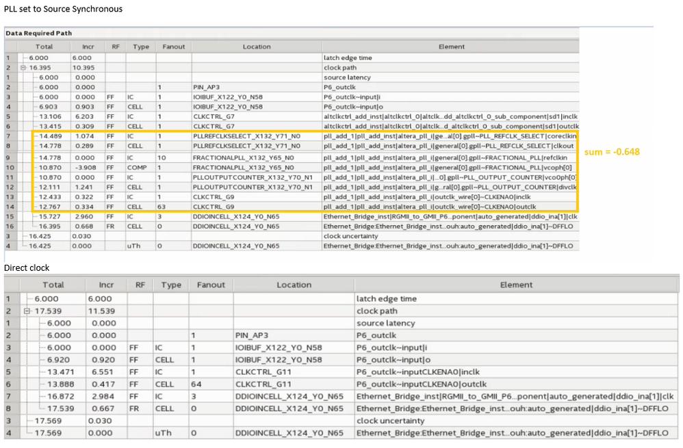
In the design you have attached, there is hold violation for some paths. The data arrival time is less than the data required time. From the screenshot above, you can see that the data required time improves a little (-0.648ns) but this is not enough. After adding the PLL, the data required time is reduced by this amount but it is still larger than the data arrival time. If you change the pin location to increase the data arrival time, you will see positive hold slack.
Thanks
Best regards,
KhaiY
Link Copied
- Mark as New
- Bookmark
- Subscribe
- Mute
- Subscribe to RSS Feed
- Permalink
- Report Inappropriate Content
Hi,
The design failed the compilation with the error below:
Error (10481): VHDL Use Clause error at mux_fpga_top.vhd(1162): design library "work" does not contain primary unit "MuxDemux_SERV". Verify that the primary unit exists in the library and has been successfully compiled.
Could you provide the design.qar file? To create the QAR file, click on Project > Archive Project > Archive
Thanks.
Best regards,
KhaiY
- Mark as New
- Bookmark
- Subscribe
- Mute
- Subscribe to RSS Feed
- Permalink
- Report Inappropriate Content
- Mark as New
- Bookmark
- Subscribe
- Mute
- Subscribe to RSS Feed
- Permalink
- Report Inappropriate Content
Hi,
Do you have the pin location finalized? Is it possible to change the pin location?
Thanks.
Best regards,
KhaiY
- Mark as New
- Bookmark
- Subscribe
- Mute
- Subscribe to RSS Feed
- Permalink
- Report Inappropriate Content
Hi,
Yes. The pinout location is finalized.
- Mark as New
- Bookmark
- Subscribe
- Mute
- Subscribe to RSS Feed
- Permalink
- Report Inappropriate Content
Hi,
I tried to change the location of the P6_outclk. There is no more timing violation on the paths. Since the location is finalized, I will try to add PLL in the design and see if the PLL can compensate the skew.
Thanks.
Best regards,
KhaiY
- Mark as New
- Bookmark
- Subscribe
- Mute
- Subscribe to RSS Feed
- Permalink
- Report Inappropriate Content
Thanks,
I tried to do that too.
IMO you won't be able to simply add a PLL. You'll probably have to path through an ALTCLKCTRL first.
- Mark as New
- Bookmark
- Subscribe
- Mute
- Subscribe to RSS Feed
- Permalink
- Report Inappropriate Content
Hi,
Yes. You are correct. I added the ALTCLKCTRL, the additional delay from ALTCLKCTRL and PLL is larger than the amount that the PLL can compensate. The delay from P6_outd[*]~input|i to Ethernet_Bridge:Ethernet_Bridge_inst|RGMII_to_GMII:RGMII_to_GMII_P6_inst|DDIO_IN_4X:M1|altddio_in:ALTDDIO_IN_component|ddio_in_ouh:auto_generated|dataout_h[*] are almost not alterable as they are located in the same I/O location. In this case, the only option is to change the pin location of P6_outclk.
Thanks.
Best regards,
KhaiY
- Mark as New
- Bookmark
- Subscribe
- Mute
- Subscribe to RSS Feed
- Permalink
- Report Inappropriate Content
"the additional delay from ALTCLKCTRL and PLL is larger than the amount that the PLL can compensate"
Can you explain this ?
Now that we're able to get the clock to the PLL - why can't we set the PLL to "normal" mode (not source synchronous) and find a phase shift that brings the PLL output clock to center alignment with the data for proper sampling ?
- Mark as New
- Bookmark
- Subscribe
- Mute
- Subscribe to RSS Feed
- Permalink
- Report Inappropriate Content
Hi,
I am sorry that I overlook the -ve sign in the calculation. The PLL does help in improving the clock path but not enough for the violation of -4.xxxns
Setting the PLL to Normal mode failed both the Setup and Hold timing.Take an example of the path in the design without PLL, the amount of setup slack is smaller than the amount of the hold violation. Shifting the latch clock does not help in this case.
From node: P6_outd[1]
To Node: Ethernet_Bridge:Ethernet_Bridge_inst|RGMII_to_GMII:RGMII_to_GMII_P6_inst|DDIO_IN_4X:M1|altddio_in:ALTDDIO_IN_component|ddio_in_ouh:auto_generated|dataout_h[1]
Setup: 3.839ns
Hold: -4.917ns
Thanks.
Best regards,
KhaiY
- Mark as New
- Bookmark
- Subscribe
- Mute
- Subscribe to RSS Feed
- Permalink
- Report Inappropriate Content
Hi,
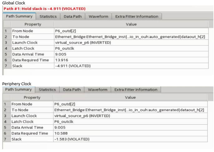
Besides this, I tried to change the P6_outclk from Global to Periphery Clock, the Clock Path improved the slack from -4.911ns to -1.583 but the violation remained. Please consider changing the location to increase the data path.
Thanks.
Best regards,
KhaiY
- Mark as New
- Bookmark
- Subscribe
- Mute
- Subscribe to RSS Feed
- Permalink
- Report Inappropriate Content
"Shifting the latch clock does not help in this case."
I have to understand this...
We have data incoming to our system and driving input DDR flip flops.
We have a clock that's connect to the wrong pin - so it's a mile away from the DDR flip flops. Indeed a problem !
BUT with a PLL - we shift the clock such that its edges are perfectly center aligned to the data.
Why center aligning the clock to the data (with a PLL) doesn't solve our problem ?
Are you saying that for some reason we won't be able to shift the clock correctly ?
Or are you saying that having the clock driving the DDR flip flop perfectly center aligned isn't enough in this case ?
- Mark as New
- Bookmark
- Subscribe
- Mute
- Subscribe to RSS Feed
- Permalink
- Report Inappropriate Content
Hi,
Shifting the latch clock does not help in this case - This refers to the path in the design without PLL.
"Take an example of the path in the design without PLL, the amount of setup slack is smaller than the amount of the hold violation. Shifting the latch clock does not help in this case."
From the report, there is setup slack of 3.839ns and hold slack of -4.917ns for the path mentioned above as an example. Setup slack of 3.839ns means the signal arrives at a time of 3.839ns earlier than what is required. Hold slack of -4.917ns means the current signal has to stay for another 4.917ns longer before the next signals comes in. If the new signal arrives the destination after another 4.917ns, the signal will fail the setup because the setup slack has only 3.839ns.
I have to understand this...
We have data incoming to our system and driving input DDR flip flops.
We have a clock that's connect to the wrong pin - so it's a mile away from the DDR flip flops. Indeed a problem !
BUT with a PLL - we shift the clock such that its edges are perfectly center aligned to the data.
Why center aligning the clock to the data (with a PLL) doesn't solve our problem ?
Are you saying that for some reason we won't be able to shift the clock correctly ?
Or are you saying that having the clock driving the DDR flip flop perfectly center aligned isn't enough in this case ?
In the design you have attached, there is hold violation for some paths. The data arrival time is less than the data required time. From the screenshot above, you can see that the data required time improves a little (-0.648ns) but this is not enough. After adding the PLL, the data required time is reduced by this amount but it is still larger than the data arrival time. If you change the pin location to increase the data arrival time, you will see positive hold slack.
Thanks
Best regards,
KhaiY
- Mark as New
- Bookmark
- Subscribe
- Mute
- Subscribe to RSS Feed
- Permalink
- Report Inappropriate Content
Hi,
May I know if you have any updates?
Thanks.
Best regards,
KhaiY
- Subscribe to RSS Feed
- Mark Topic as New
- Mark Topic as Read
- Float this Topic for Current User
- Bookmark
- Subscribe
- Printer Friendly Page

