- Mark as New
- Bookmark
- Subscribe
- Mute
- Subscribe to RSS Feed
- Permalink
- Report Inappropriate Content
I'm using Quartus-II Rev. 18.1 in order to program .jic file into ISSI IS128LP128 flash memory at active serial mode, but without success.
1). How should I connect IS128LP128 (8-pins) to Cyclone-V-GX?
Do you have an example ?
Where should be connected pin ASDO of the FPGA-to SI of the flash?
2). ISSI flash components are absent from "Configuration Device" Tab.
What option should I choose instead?
Link Copied
- Mark as New
- Bookmark
- Subscribe
- Mute
- Subscribe to RSS Feed
- Permalink
- Report Inappropriate Content
Hi AGofs,
You may refer to this solution here:
https://forums.intel.com/s/feed/0D50P00004ImOLLSA3
-------------------------------------------------------------------------------------
CBATT (Customer)
a month ago
Hi,
I believe that this problem may be solved. If not, here on how we manage to get this memory to work with Quartus 19.1 for write, erase and FPGA initialization.
- Open Programmer
- Go to File > Convert Programming File
- Programming file type, select .jic
- Open configuration device using "..."
- Select your device family
- Create a <<new device>>
- Configure according to your memory datasheet
- e.g., name: IS25LP128, ID: 17, Density: 128Mb, Single dummy: 8, Quad dummy: 6
- Select Micron as Flow template
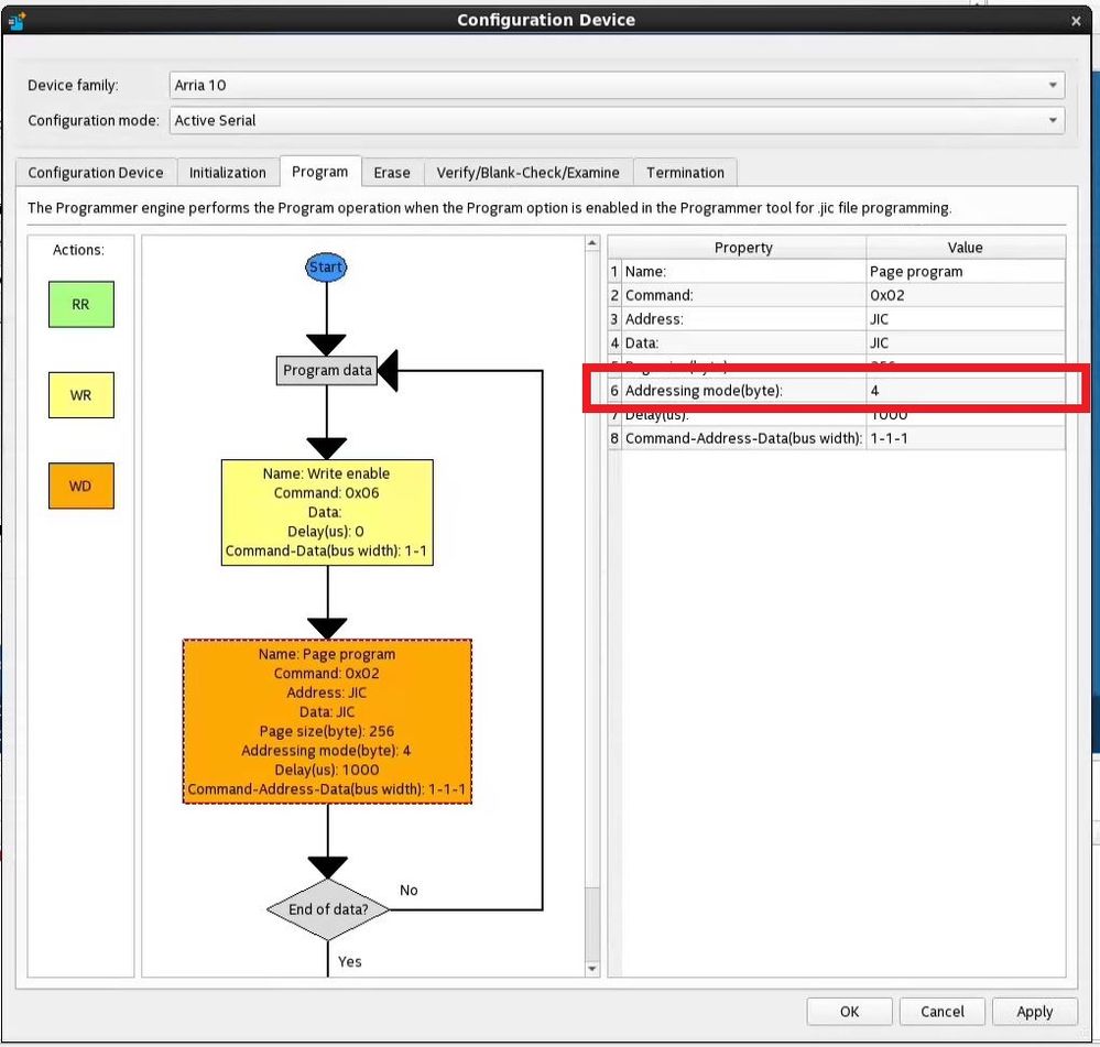
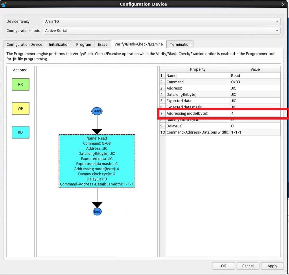
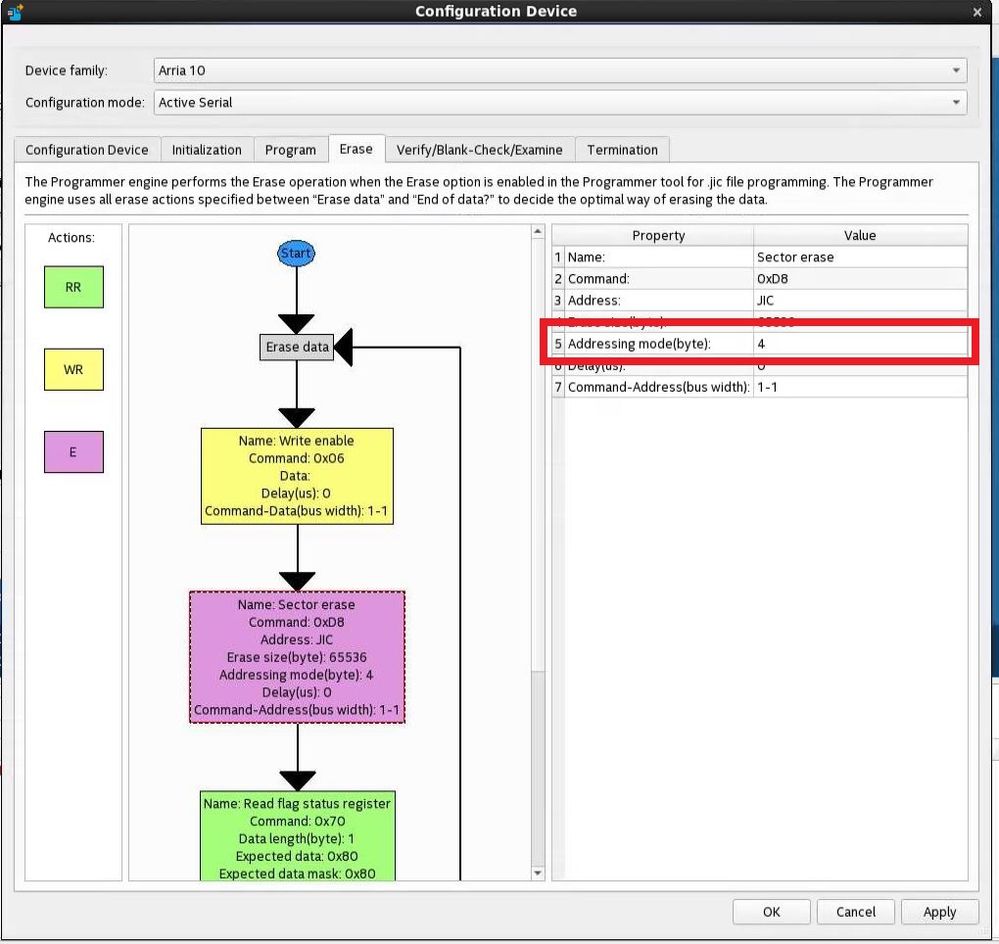
- Change Addressing mode(byte) from each flow tab from 4 to 3
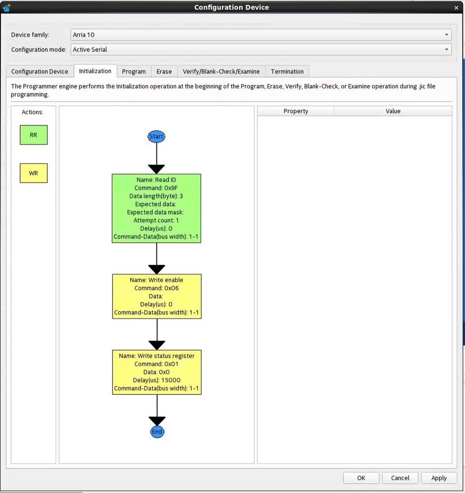
- In initialization tab:
- Remove everything except Read ID (Command 0x9F), Write Enable (Command 0x06) and Write status register (Command 0x01), keep this flow order
- Note that you need a Write Enable before sending other commands, check your memory datasheet for more info
- In erase tab:
- Change Read flag status register to Read status register
- Change Command to 0x05 (ISSI memory uses the READ STATUS REGISTER OPERATION for erase status)
- Change Expected data to 0x00
- Change Expected data mask to 0x01
I hope this helps.
×
-------------------------------------------------------------------------------------
- Mark as New
- Bookmark
- Subscribe
- Mute
- Subscribe to RSS Feed
- Permalink
- Report Inappropriate Content
- Mark as New
- Bookmark
- Subscribe
- Mute
- Subscribe to RSS Feed
- Permalink
- Report Inappropriate Content
Hi AGofs,
This feature only available starting 18.1.1 Standard version or 19.1 pro version.
- https://www.intel.com/content/dam/www/programmable/us/en/pdfs/literature/ug/ug-qps-gen-flash-programmer.pdf
- https://www.intel.com/content/dam/www/programmable/us/en/pdfs/literature/ug/archives/ug-qpp-gen-flash-programmer-19-1.pdf
I dont think it is possible using 18.1 lite edition.
i'm apologize for any inconvenience.
Thanks
- Mark as New
- Bookmark
- Subscribe
- Mute
- Subscribe to RSS Feed
- Permalink
- Report Inappropriate Content
- Mark as New
- Bookmark
- Subscribe
- Mute
- Subscribe to RSS Feed
- Permalink
- Report Inappropriate Content
- Mark as New
- Bookmark
- Subscribe
- Mute
- Subscribe to RSS Feed
- Permalink
- Report Inappropriate Content
Hi AGofs,
During configuration I saw the row named "Total Device die".
What should I write in this row?
IS25LP128 do not have stack die. then you should write it as 1.
if MT25QU01G device, it have 2 stacked die. Thus, MT25QU01G should write as 2.
You wrote at point 9 :"Change Addressing mode(Byte)….).
Where is it?
Every tab (Program, Erase, Verify... tab) you need to change address byte from 4 to 3.
As I understand you , only 3 commands must remain: Read ID=>Write enable=>Write Status Register.
Every another command from Initialization Tab must be removed .
Am I right?
Yes, you're right
I'm apologize for delay reply. I'm on Christmas & New Year holiday.
Cheers
- Mark as New
- Bookmark
- Subscribe
- Mute
- Subscribe to RSS Feed
- Permalink
- Report Inappropriate Content
Thank you very much WolfGang.
I've produced .jic successfully.
You can close the case.
Happy New Year!
- Mark as New
- Bookmark
- Subscribe
- Mute
- Subscribe to RSS Feed
- Permalink
- Report Inappropriate Content
- Subscribe to RSS Feed
- Mark Topic as New
- Mark Topic as Read
- Float this Topic for Current User
- Bookmark
- Subscribe
- Printer Friendly Page


