- Mark as New
- Bookmark
- Subscribe
- Mute
- Subscribe to RSS Feed
- Permalink
- Report Inappropriate Content
Hello,
Probably I didn't properly define timing constraints ... TimeQuest reported quite a lot of timing violations. In this connection I have one question - does exist some straightforward approach on working around "timing violations" ? For example on the image below there are 2 screenshots form TimeQuest:- top screenshot - results of "Report Top Failing Paths"
- bottom screenshot - "Peport Timing" for the path, highlighted in yellow on the top screenshot
.jpg)
Link Copied
- « Previous
-
- 1
- 2
- Next »
- Mark as New
- Bookmark
- Subscribe
- Mute
- Subscribe to RSS Feed
- Permalink
- Report Inappropriate Content
--- Quote Start --- No, according to SDRAM datasheet, it's clocked on positive edge. So, you propose to remove phase shift on u0|pll|altera_pll_i|general[1].gpll~PLL_OUTPUT_COUNTER|divclk and consequently on clk_ext_sdram ? --- Quote End --- For an SDR interface try first same phase and if you get into trouble then play with the phase.
- Mark as New
- Bookmark
- Subscribe
- Mute
- Subscribe to RSS Feed
- Permalink
- Report Inappropriate Content
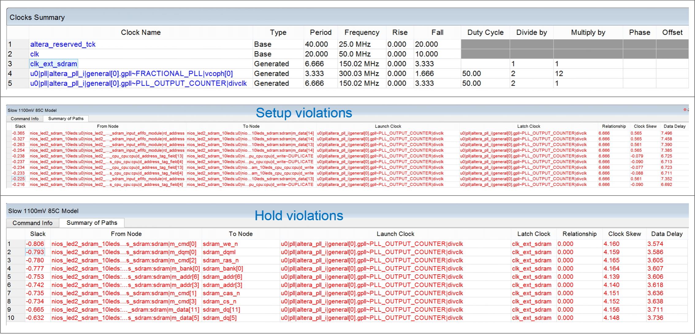
Here is TimeQuest results with no phase shift between 2 PLL-derived clocks:
- 1st clcok clocks all Qsys modules (including SDRAM controller)
- 2nd clock clocks external SDRAM chip
- Report Clocks
- Report Timing SETUP "to clock" u0|pll|altera_pll_i|general
- Report Timing HOLD "to clock" clk_ext_sdram
- Mark as New
- Bookmark
- Subscribe
- Mute
- Subscribe to RSS Feed
- Permalink
- Report Inappropriate Content
You better run TimeQuest GUI and check all failing paths and io paths.
Your setup report seems about internal paths [launch and latch are divclk] but your hold report is io path which shows some negative slack. You need to check setup for io paths as well. Both inputs and output io paths need to be reported. If io paths are failing you can use some phase shift to help it out [you can experiment on that]. For internal paths on 150MHz that is a design issue and basically 150MHz should not be a problem in many fpgas. But it is not clear why this failure occurs.- Mark as New
- Bookmark
- Subscribe
- Mute
- Subscribe to RSS Feed
- Permalink
- Report Inappropriate Content
--- Quote Start --- You better run TimeQuest GUI and check all failing paths and io paths. --- Quote End --- It's the case, I generated these reports in TimeQuest GUI. I've just run failing paths - 200 violations (I suppose it's maximum that can be displayed, probably there are more ...) --- Quote Start --- Your setup report seems about internal paths [launch and latch are divclk] but your hold report is io path which shows some negative slack. You need to check setup for io paths as well. Both inputs and output io paths need to be reported. --- Quote End --- Ok, I did it - there are no violations in "Report All I/O Timings" --- Quote Start --- If io paths are failing you can use some phase shift to help it out [you can experiment on that]. For internal paths on 150MHz that is a design issue and basically 150MHz should not be a problem in many fpgas. But it is not clear why this failure occurs. --- Quote End --- Do you mean here "Report All I/O Timings" ?
- Mark as New
- Bookmark
- Subscribe
- Mute
- Subscribe to RSS Feed
- Permalink
- Report Inappropriate Content
I would have thought that io failed hold time based on my reading in your second report as it is launch by divclk but latch by clk_ext_sdram.
So how could io report pass with no failure. Obviously I am mis-reading your reports. You are in a position to identify if io paths are ok. If so no need fr phase shift and your focus should be on the design. issues like using fitter settings, pipelining if available...I know it is qsys generated stuff but you can manipulate settings.- Mark as New
- Bookmark
- Subscribe
- Mute
- Subscribe to RSS Feed
- Permalink
- Report Inappropriate Content
Ok, I'll try to "decorticate" Qsys-generated staff ... not sure it will be simple, taking into account that I'm not quite comfortable with TimeQuest.
--- Quote Start --- I would have thought that io failed hold time based on my reading in your second report ... --- Quote End --- Do you mean my 2nd message on this thread ? The design was modified since that moment ... e.g. 2 PLL outputs became in phase.- Mark as New
- Bookmark
- Subscribe
- Mute
- Subscribe to RSS Feed
- Permalink
- Report Inappropriate Content
--- Quote Start --- Do you mean my 2nd message on this thread ? The design was modified since that moment ... e.g. 2 PLL outputs became in phase. --- Quote End --- I meant this last post from you: Report Timing HOLD "to clock" clk_ext_sdram It could be the clk_ext_sdram is latching e.g. m_dq to sdram_dq internally then sending it to sdram. But I thought you have defined clk_ext_sdram as generated output clock.
- Mark as New
- Bookmark
- Subscribe
- Mute
- Subscribe to RSS Feed
- Permalink
- Report Inappropriate Content
Looking at the path for the clock going out to SDRAM and data coming back. Let's start with the case where you use the same clock to launch and latch the data, so there is a 0ns hold relationship and 7.5ns setup. Let's say the external delay -max and -min are both 0ns. If you compile and your setup slack is 1ns and your hold slack is 3ns. To think of what's going on, let's say the clock skew is 0 inside the FPGA. (This is weird, as the clock feeds the latch register, but it doesn't feed an actual launch register. Let's just say it's the output register). Anyway, by having 1ns of setup slack, it means the clock got out through the output buffer and came back in through the data input buffer and to the register in 6.5ns. So your max data delay is 6.5ns.
By having 3ns of hold slack, we're saying this same delay in the Fast Timing Model was 3ns. Of course, your external delay is not 0ns. Let's say the SDRAM's TCO has a max of 8ns and min of 4ns. So if you change the external delays to this, with the same fit, you would end up with setup slack of -7ns and hold slack of 7ns. So we're missing timing by a lot. You could add a multicycle setup of 2 and multicycle hold of 1, so that your now trying to latch on the next falling edge at time 15ns, e.g. when a clock edge comes in at time 0ns, it will go out of the FPGA to the SDRAM, have data come back, and you'll latch that at time 15ns. You will also have a positive hold relationship of 7.5ns, meaning that whole delay must be greater than 7.5ns. Since your FPGA delay was 6ns and you added 8ns for the external delay, the total is 14ns and your actually making setup. But your fastest delay is 7ns and you need it to be 7.5ns. THis is where it gets tricky, as the fitter can turn up delay chains/routing to try and meet hold. But let's say it adds 0.75ns of delay and now it's meeting hold in the Fast Corner. As a general rule of thumb, I say the slow corner is 2x the Fast Corner, so this would add 1.5ns of delay to the slowest delay, e.g the FPGA data path becomes 6+1.5=7.5ns and then with the 8ns external delay you're now failing setup rlationship 15ns. This is just an example, but you do need to figure out the external delays because I don't know if you're in the right ballpark of whether this is feasible, as 150MHz is pretty fast for SDRAM interface. Now, it may be that you don't read on every cycle, e.g. it may be every other cycle at best. In that case, your setup relatinoship could be 15ns but your hold could be 0ns, in which case the fitter would never need to add delay to meet hold timing, as it would automatically meet the hold.- Mark as New
- Bookmark
- Subscribe
- Mute
- Subscribe to RSS Feed
- Permalink
- Report Inappropriate Content
Ryan, first thank you for explanation.
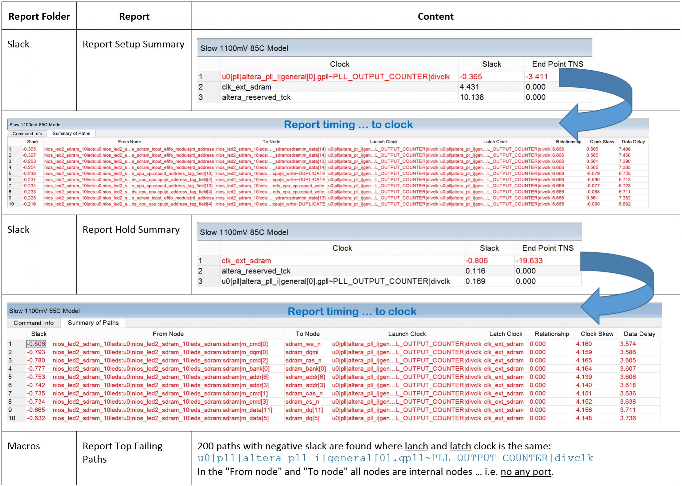
Nevertheless, I remains a little bit confused. Primary question - "What to start with ?" timequest generates multitude of different reports ... What report to start with ? I passed trough all selected those with timing violations. Here below the short resume of timing violations output by TimeQuest: https://www.alteraforum.com/forum/attachment.php?attachmentid=13619 There are 3 "sections", where I've found timing violations:- Summary (Setup), where violations are related to the clock ...divclk. Time report "To clock" followed divclk and revealed 10 violations
- Summary (Hold), where violations are related to the clock clk_ext_sdram. Time report "To clock" followed clk_ext_sdram and also revealed 10 violations
- Report failing path - revealed 200 violations, realted to ...divclk for both launch and latch clocks and nodes are internal, i.e. no external ports
- Mark as New
- Bookmark
- Subscribe
- Mute
- Subscribe to RSS Feed
- Permalink
- Report Inappropriate Content
I'm using a SDRAM at 100 MHz clock whit the SDRAM controller in QSYS (altera_avalon_new_sdram_controller). For calculation the shift between the controller clock and the external clock I used the Embedded Peripherals IP User Guide (UG-01085 2016.12.19, page 2-10).
In the .sdc I defined a setup multicycle for shifting the window: set_multicycle_path -from [get_clocks SOPC|sys_pll|clk_100] -to [get_clocks virt_100MHz_clk] -setup 2 These clock groups must related in timequest, do not use set_clock_groups -asynchronous/ -exclusive. Here you is a good guidance for this toic: http://retroramblings.net/?p=515 regards Jens- Mark as New
- Bookmark
- Subscribe
- Mute
- Subscribe to RSS Feed
- Permalink
- Report Inappropriate Content
Hi Jens,
A couple of questions:- Did you apply multicycle constraint at once ... or after running TimeQuest (and analyzing results) at least one time ?
- What is virt_100mhz_clk? Is it external clock or PLL-generated clock ?
- Did you try to workaround timing violations by tuning the phase shift between "sdram clock" and "sdram controller clock" ?
create_clock -name clk -period 20 create_clock -name {altera_reserved_tck} -period 40 {altera_reserved_tck}
derive_pll_clocks
derive_clock_uncertainty
set_input_delay -clock altera_reserved_tck -clock_fall 3
set_input_delay -clock altera_reserved_tck -clock_fall 3
set_output_delay -clock altera_reserved_tck 3
create_generated_clock -name clk_ext_sdram -source .gpll~PLL_OUTPUT_COUNTER|divclk}]
#  Constraint SDRAM DATA for input
set_input_delay -clock clk_ext_sdram -max 6.4 ]
set_input_delay -clock clk_ext_sdram -min 1.0 ]
#  Constraint SDRAM DATA for output
set_output_delay -clock clk_ext_sdram -max 1.5
set_output_delay -clock clk_ext_sdram -min -0.8
set_multicycle_path -setup -to }] 2# set_multicycle_path -hold -to }] 1
set_false_path -from
set_false_path -from
set_false_path -from * -to
set_false_path -from * -to
The 1st location where I consult timing violations is "Report all I/O Timings". There are 16 timing HOLD violations (related to SDRAM data) and 55 SETUP violations (related to all (at 1st glance) SDRAM ports). Surprisingly launch clock and latch clock are the same. Any comments. Thanks. Here is screenshot for HOLD violations. https://alteraforum.com/forum/attachment.php?attachmentid=13664&stc=1
- Mark as New
- Bookmark
- Subscribe
- Mute
- Subscribe to RSS Feed
- Permalink
- Report Inappropriate Content
Hi Pavel,
1. Yes at once becaus the fitter is using timing constraints. 2. It's the virtual clock for the I/O timing analysis (see Quartus II Handbook, QII5V3 2015.05.04. p. 7-14 or the TimeQuest User guide from Ryan Scoville, http://www.alterawiki.com/wiki/timequest_user_guide) 3. No, I use the shift calculated according the Embedded Peripherals IP User Guide Do you drive the internal sdram_controller with the same clock as the external SDRAM device? The external clocks should be shifted. In your screenshot the launch clock should be the external shifted clock and the latch clock is the internal clock. The multicycle -setup constraint is used to tell Timequest what is the right latch edge.- Mark as New
- Bookmark
- Subscribe
- Mute
- Subscribe to RSS Feed
- Permalink
- Report Inappropriate Content
Hi Jens,
1. yes at once becaus the fitter is using timing constraints. Well ... this is probably a critical point that I fail to understand: after all timing relations e.g. clock/clock, clock/interface signal are influenced by routing. Here I mean that fitter can be quite "smart" and will route all tracks so that NONE adjusting with PLL clock shifting or multicycle is necessary. But this can be known AFTER fitting is run at least one time. Or I missed something ? 2. it's the virtual clock for the i/o timing analysis (see quartus ii handbook, qii5v3 2015.05.04. p. 7-14 or the timequest user guide from ryan scoville, http://www.alterawiki.com/wiki/timequest_user_guide) In these two sources virtual clock is created because it's external (i.e. generated OUTSIDE FPGA) whereas on my board both "SDRAM clock" and "SDRAM controller clock" are generated INSIDE FPGA. Is it also your case ? 3. no, i use the shift calculated according the embedded peripherals ip user guide Ok, but I meant something other. It seems that in the "Embedded Peripherals IP User Guide" this shift is used to setup phase shift between 2 clocks, generated by PLL and it's the ONLY remedy against timing violations ... because they don't mention multicyling. My question was about eventual possibility to use ONLY phase shift for timing violation workaround (without any multicycling). Did you try this ? do you drive the internal sdram_controller with the same clock as the external sdram device? the external clocks should be shifted. No, they are driven by 2 clocks. These 2 clocks are PLL-generated and shifted one relative to other according to "Embedded Peripherals IP User Guide" procedure. in your screenshot the launch clock should be the external shifted clock and the latch clock is the internal clock. That is strange because clk_ext_sdram is actually u0...divclk. the multicycle -setup constraint is used to tell timequest what is the right latch edge. I considered that timequest is quite "smart" and capable to deduct it itself. After all, multicycle option isn't mandatory, how TimeQuest manage this if there is no multicycling. Thanks once more.- Mark as New
- Bookmark
- Subscribe
- Mute
- Subscribe to RSS Feed
- Permalink
- Report Inappropriate Content
1. If you look at the fitter messages you can see something like this:
"Info (332104): Reading SDC File: 'project_timing.sdc'" I think fitter use constraints for controlling desing optimization. 2. The virtual clock is just used outside the FPGA. No internal logic is driven from this clock but it's from the PLL inside. 3. Yes I do. Sometimes it works. But if you want closure timing than you have to use the rigth constraints. Jens- Mark as New
- Bookmark
- Subscribe
- Mute
- Subscribe to RSS Feed
- Permalink
- Report Inappropriate Content
1. Sure, it does. But once again, when you are starting to work with your design and didn't run TimeQuest, how can you know beforehand that multicycle constraint is necessary for this particular design ?
At the beginning you have no any information how your design will be fit, isn't it ? I perceive applying timing constraint as "iterative" process: when starting with design the timing constraints should be as relaxed as possible ... only the mandatory ones (e.g. create_clock, etc.) Then, running TimeQuest and analyzing results, you apply additional constraints (e.g. multicycling) if necessary to get finally your design without timing violations. But applying multicycling "at once", without any feedback from TimeQuest ... frankly speaking I don't understand. 2. So, on your board the SDRAM chip is clocked by an external clock, and NOT by one, coming from FPGA ? 3. So, first you try to resolve timing issues using shift between two PLL-generated clocks and when this shift isn't sufficient, you use multicycling. Correct ? Here I didn't understand one thing: if you use (like me) two PLL-generated clocks (one - for SDRAM chip, other - for SDRAM controller), what is usage of virtual clock ? What it clocks exactly ?- Mark as New
- Bookmark
- Subscribe
- Mute
- Subscribe to RSS Feed
- Permalink
- Report Inappropriate Content
Pavel, you are rigth constrain timing is an iterative process.
No the SDRAM is clocked from the FPGA. As I wrote the clock does not drive any internal logic but it comes from an internal PLL. This virtual clock is used to constrain the I/O timing like: set_output_delay -max $SDRAM_MAX_OUT_DELAY -clock virt_100MHz_clk [get_ports SD_DATA*] Jens- Mark as New
- Bookmark
- Subscribe
- Mute
- Subscribe to RSS Feed
- Permalink
- Report Inappropriate Content
--- Quote Start --- Pavel, you are rigth constrain timing is an iterative process --- Quote End --- So, you confirm that when you start working on your project (i.e. design is accomplished in Quartus/Qsys, but isn't compiled yet), you have no any idea how how design will be fit during compilation. Consequently you can't apply any "hard" constraints (e.g. multicycling), but only the very basic ones (i.e. creating clocks), isn't it ? That's why I was surprised when you said that you apply "multicycling" constraint "at once" (i.e. without preliminary compilation or TimeQuest run). Or I misunderstood your approach ? --- Quote Start --- No the SDRAM is clocked from the FPGA. As I wrote the clock does not drive any internal logic but it comes from an internal PLL. --- Quote End --- If you have no any additional clocks on your board (except basic clock), what sense to create virtual clock ? In all manuals virtual clock is created to "emulate" some external clock. --- Quote Start --- This virtual clock is used to constrain the I/O timing like: set_output_delay -max $SDRAM_MAX_OUT_DELAY -clock virt_100MHz_clk [get_ports SD_DATA*] --- Quote End --- Why not use PLL-generated clock for this ?
- Mark as New
- Bookmark
- Subscribe
- Mute
- Subscribe to RSS Feed
- Permalink
- Report Inappropriate Content
I use all timing constraints in every synthesis run (not just for timing analysis with Timequest). Finding the right ones it's an iterative process. Before you can run Timequest you have to do a complete fit. First I assign basic constraints (base clocks, virtual clocks, I/O delays, derive_pll_clocks, derive_clock_uncertainty, set_clock_groups)
The virtual clocks are for I/O timing analysis, please refer TimeQuest Timing Analyzer Cookbook (MNL-01035 2016.2.25, page 9) Jens- Mark as New
- Bookmark
- Subscribe
- Mute
- Subscribe to RSS Feed
- Permalink
- Report Inappropriate Content
For internal paths on 150MHz that is a design issue and basically 150MHz should not be a problem in many fpgas.
- Subscribe to RSS Feed
- Mark Topic as New
- Mark Topic as Read
- Float this Topic for Current User
- Bookmark
- Subscribe
- Printer Friendly Page
- « Previous
-
- 1
- 2
- Next »