- Отметить как новое
- Закладка
- Подписаться
- Отключить
- Подписка на RSS-канал
- Выделить
- Печать
- Сообщить о недопустимом содержимом
I keep getting violations (negative slack) in the timing analyzer on the 1200mV 0°C "fast" model, the other models are fine.
These are the violations it reports: -0.055 0.078 0.184 0.051 Low Pulse Width clk Rise old -0.055 0.078 0.184 0.051 Low Pulse Width clk Rise temp What does this "low pulse width" refer to? I'm concerned because I need the design to work below 0°C. I am using Quartus II 8.0SP1 and my VHDL code is as follows: PROCESS (rst, clk) BEGIN IF (rst='1') THEN temp <= '0'; old <= '0'; ELSIF (clk'EVENT AND clk='1') THEN old <= temp; temp <= d; END IF; END PROCESS;Ссылка скопирована
- Отметить как новое
- Закладка
- Подписаться
- Отключить
- Подписка на RSS-канал
- Выделить
- Печать
- Сообщить о недопустимом содержимом
This TimeQuest report includes both the pulse-width specs and toggle-rate specs documented in the device handbook. I don't remember which term is used in the table for each spec in the handbook, but "pulse width" might be the pulse-width spec for the type of global routing being used.
- Отметить как новое
- Закладка
- Подписаться
- Отключить
- Подписка на RSS-канал
- Выделить
- Печать
- Сообщить о недопустимом содержимом
With the same model I also observed the problem with Modelsim-AE. When d changes state right before a clock edge, temp goes into state X (unknown).
http://www.foo.is/albums/misc/timingviolation.sized.png (http://www.foo.is/albums/misc/timingviolation.png) Is there a way around this?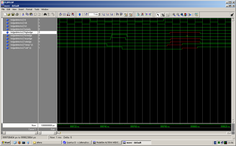
- Отметить как новое
- Закладка
- Подписаться
- Отключить
- Подписка на RSS-канал
- Выделить
- Печать
- Сообщить о недопустимом содержимом
Looking at this simulation, I'm not even sure it is a problem. A pulse on input d is guaranteed to last a long time (more than a few clocks) and since signals never go unkown in a real device, if d is incorrectly read at the first clock after a state change on d, it'll just be processed correctly one clock later, which is a non-issue in this application as I have more than enough resolution in my clock rate vs the d signal.
It does serve as a reminder to oversample signals like this enough to not miss a pulse.- Отметить как новое
- Закладка
- Подписаться
- Отключить
- Подписка на RSS-канал
- Выделить
- Печать
- Сообщить о недопустимом содержимом
From my point of view it looks like a standard setup/hold violation. The d input is raised only about 1 ns before the clock edge. If you are sure that this is not an issue then you might apply a false_path assigngment to this pin.
- Отметить как новое
- Закладка
- Подписаться
- Отключить
- Подписка на RSS-канал
- Выделить
- Печать
- Сообщить о недопустимом содержимом
Since the d input comes from another clock domain, of course I cannot guarantee it's timing with relation to the clock, I do however have the guarantee that d is so much slower that a jitter of more than a full clock cycle is no issue. I will see if that change silences the warnings in the simulator.
- Отметить как новое
- Закладка
- Подписаться
- Отключить
- Подписка на RSS-канал
- Выделить
- Печать
- Сообщить о недопустимом содержимом
Minimum pulse width errors won't show up in the simulation. If d is coming from another domain, then at some time you will violate the setup or hold of the receive register, and that register will go metastable, so be sure your design handles that(add one or two more registers to de-metastabilize it). If you want the register to not go to X in the simulation, then in the Assignment Editor apply the setting "Show X on Violation" to Off for that register.
- Отметить как новое
- Закладка
- Подписаться
- Отключить
- Подписка на RSS-канал
- Выделить
- Печать
- Сообщить о недопустимом содержимом
--- Quote Start --- Minimum pulse width errors won't show up in the simulation. If d is coming from another domain, then at some time you will violate the setup or hold of the receive register, and that register will go metastable, so be sure your design handles that(add one or two more registers to de-metastabilize it). If you want the register to not go to X in the simulation, then in the Assignment Editor apply the setting "Show X on Violation" to Off for that register. --- Quote End --- Ok, so it is possible for a register in an FPGA to store a value that is neither 0 nor 1?
- Отметить как новое
- Закладка
- Подписаться
- Отключить
- Подписка на RSS-канал
- Выделить
- Печать
- Сообщить о недопустимом содержимом
It's not storing the value. It's more that it gets stuck switching, and takes an unkown amount of time to resolve itsef. The classical picture on metastability is a hill with 1 and 0 on both sides, and a ball that is pushed over the hill to switch between 1 and 0. But when the uTsu or uTh is violated, that ball gets pushed to the top of the hill but doesn't have the momentum to go to the other side, and so it takes longer for it eventually roll back down(and you don't know which way it will roll). That's why more registers are added, so that they have a period of time to wait for that ball to roll to a valid state before the clock it. Otherwise, if the unkown state is sent out to multiple registers, one might see it and resolve it as a 1, while another may resolve it to be a 0, and when different registers identify the same signal as different values, bad things can happen(state-machin lockup, etc.).
But in simulation, when a register's uTsu and uTh is violated, that register goes to X and never gets resolved. So that X propogates throughout the design and the simulation is essentially useless. So you add this assignment saying not to go to X but to a 1 or a 0(doesn't matter which, since physically you never know) and the simulation will work. Naturally, this is a brief description. In TimeQuest for Stratix III, thre is a metastability analysis(has to be enabled under Fitter Settings)- Отметить как новое
- Закладка
- Подписаться
- Отключить
- Подписка на RSS-канал
- Выделить
- Печать
- Сообщить о недопустимом содержимом
Thank you for the explanation. I had previously learned that I should latch incoming signals that are fed to more than one input. The purpose of this part of the design is just to find edges in the incoming signal and create a clock-enable signal that lasts for one clock and enables a lot of different processes that do calculations based on the edges of this input signal.
- Подписка на RSS-канал
- Отметить тему как новую
- Отметить тему как прочитанную
- Выполнить отслеживание данной Тема для текущего пользователя
- Закладка
- Подписаться
- Страница в формате печати