- Mark as New
- Bookmark
- Subscribe
- Mute
- Subscribe to RSS Feed
- Permalink
- Report Inappropriate Content
Hello,
TimeQuest Analyzer reported 63 "Setup" violations, and all of them are located on internal nodes. Does exist some strategy to fix internal nodes timing violations, e.g. add some constraints in .sdc file ? Thanks.Link Copied
4 Replies
- Mark as New
- Bookmark
- Subscribe
- Mute
- Subscribe to RSS Feed
- Permalink
- Report Inappropriate Content
What do you mean by "internal nodes"? Internal to what?
Setup violations usually occur because there is too much logic between registers. The easiest fix is to add extra pipeline stages on these paths in your HDL.- Mark as New
- Bookmark
- Subscribe
- Mute
- Subscribe to RSS Feed
- Permalink
- Report Inappropriate Content
--- Quote Start --- What do you mean by "internal nodes"? Internal to what? Setup violations usually occur because there is too much logic between registers. The easiest fix is to add extra pipeline stages on these paths in your HDL. --- Quote End --- Thanks Tricky, I mean "internal-to-internal". Here is "Top Failing Paths": https://www.alteraforum.com/forum/attachment.php?attachmentid=14179 These paths come from from sdram controller IP. add extra pipeline stages ... you mean edit IP code ?
- Mark as New
- Bookmark
- Subscribe
- Mute
- Subscribe to RSS Feed
- Permalink
- Report Inappropriate Content
If its in an IP, then no, you generally cannot edit it.
Are you sure the constraints are correct and not too fast? How full is the device? Have you tried a different fitter seed?- Mark as New
- Bookmark
- Subscribe
- Mute
- Subscribe to RSS Feed
- Permalink
- Report Inappropriate Content
Correct or not, I'm not sure ... at least there is no ignored constraints.
Concerning input/output delay, they were generated by the project builder - utility, delivered by board manufacturer - Terasic. BTW, here is the content of constraint file:#**************************************************************
# This .sdc file is created by Terasic Tool.
# Users are recommended to modify this file to match users logic.
# **************************************************************
# **************************************************************
# Create Clock
# **************************************************************
create_clock -period 20.0 -name clk CLOCK_50
# for enhancing USB BlasterII to be reliable, 25MHz
create_clock -name {altera_reserved_tck} -period 40 {altera_reserved_tck}
derive_pll_clocks
derive_clock_uncertainty
set_input_delay -clock altera_reserved_tck -clock_fall 3
set_input_delay -clock altera_reserved_tck -clock_fall 3
set_output_delay -clock altera_reserved_tck 3
# **************************************************************
# Create Generated Clock
# **************************************************************
create_generated_clock -name clk_sdram_ext -source .gpll~FRACTIONAL_PLL|fbclk}]
create_generated_clock -name clk_data -source .gpll~PLL_OUTPUT_COUNTER|divclk}] |clk}]
# **************************************************************
# Set Input Delay
# **************************************************************
# Board Delay (Data) + Propagation Delay - Board Delay (Clock)
set_input_delay -clock clk_sdram_ext -max -0.048
set_input_delay -clock clk_sdram_ext -min -0.057
# **************************************************************
# Set Output Delay
# **************************************************************
# max : Board Delay (Data) - Board Delay (Clock) + tsu (External Device)
# min : Board Delay (Data) - Board Delay (Clock) - th (External Device)
set_output_delay -clock clk_data -max 1.452
set_output_delay -clock clk_data -min -0.857
set_output_delay -clock clk_data -max 1.531
set_output_delay -clock clk_data -min -0.805
set_output_delay -clock clk_data -max 1.533
set_output_delay -clock clk_data -min -0.805
set_output_delay -clock clk_data -max 1.510
set_output_delay -clock clk_data -min -0.800
set_output_delay -clock clk_data -max 1.520
set_output_delay -clock clk_data -min -0.780
set_output_delay -clock clk_data -max 1.5000
set_output_delay -clock clk_data -min -0.800
set_output_delay -clock clk_data -max 1.545
set_output_delay -clock clk_data -min -0.755
set_output_delay -clock clk_data -max 1.496
set_output_delay -clock clk_data -min -0.804
set_output_delay -clock clk_data -max 1.508
set_output_delay -clock clk_data -min -0.792
# **************************************************************
# Set Clock Groups
# **************************************************************
# **************************************************************
# Set False Path
# **************************************************************
set_false_path -from
set_false_path -from
set_false_path -from * -to
set_false_path -from * -to
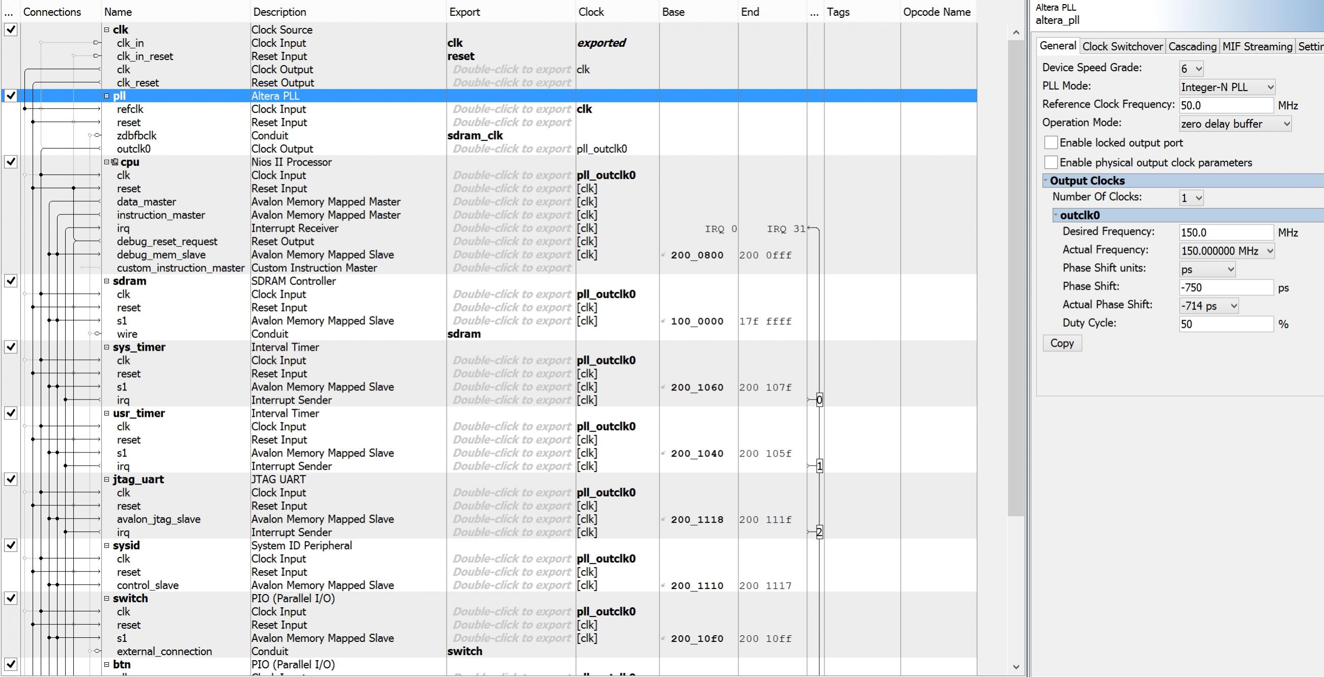
set_false_path -from * -to clk_data - output of the "zero delay buffer" PLL, clk_sdram_ext - zdbfbclk output of the same PLL that is applied to the external SDRAM clock input. I'm not sure that such connection solution is perfect - I picked it from old Altera presentation (at least as I understood it) https://www.alteraforum.com/forum/attachment.php?attachmentid=14180
Reply
Topic Options
- Subscribe to RSS Feed
- Mark Topic as New
- Mark Topic as Read
- Float this Topic for Current User
- Bookmark
- Subscribe
- Printer Friendly Page