- Mark as New
- Bookmark
- Subscribe
- Mute
- Subscribe to RSS Feed
- Permalink
- Report Inappropriate Content
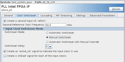
I have a design were I am trying to use the Input Clock MUX to Switch between two input pin clock ports. The PLLs are in platform designer and I get the following warning:
Warning: test_system_qsys.pll_26_104.refclk1: Signal refclk1 has unknown type refclk1.
Now the two clock pins already pass through the clock_source IP blocks on the way to the PLL. The PLL has 2 reference clocks in which I have programmed "manual" switching. No matter which clock I put on refclk1 I get the same warning and the result is the second clock is NOT PRESENT at the input of the PLL after fitting as examined in the technology view.
Both clocks are signal ended and arriving on dedicated clock input pins. Both clocks are on the bottom of the die.
I am using Quartus Prime 21.1 build 842. This is for an Arrai5 GX device which is on your Arria5GX Reference board.
Upon further review the manual switchover and activeclk signal are also not present on the PLL in post fit technology view???
Any guidance would be welcome,
TomT...
Link Copied
- Mark as New
- Bookmark
- Subscribe
- Mute
- Subscribe to RSS Feed
- Permalink
- Report Inappropriate Content
Kindly note that there will be some slowness on the first reply due to the public holiday, we will get back to you as soon as possible.
- Mark as New
- Bookmark
- Subscribe
- Mute
- Subscribe to RSS Feed
- Permalink
- Report Inappropriate Content
Hi,
Thank you for using Intel's support services. Can you provide your project so that we can help you locate the problem?
Thanks & Regards,
Tingjiang
- Mark as New
- Bookmark
- Subscribe
- Mute
- Subscribe to RSS Feed
- Permalink
- Report Inappropriate Content
Unfortunately I cannot provide you the project because of company policy. Here are the details:
clkin_50_bot pin_AP20
hsma_clk_in0 pin_AL5
PLL configured in the Platform Designer with the following behavior:
refclk1 = clkin_50_bot, passes through Clock Source IP
refclk = hsma_clk_in0, passes through Clock Source IP
Configured to use Manual Clock Switchover
PLL creates:
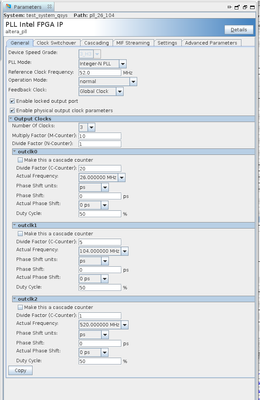
outclk0 = 26MHz
outclk1 = 104MHz
outclk2 = 520MHz
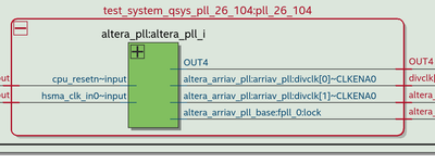
Once I have created this design through compile I use the Netlist View -> Post Fitter to get the following schematic view:
As you can see only one of the input clocks? Also notice that I don't have the manual clock switching output or the output which tells me which clock is being used. The only "warning" I receive is the following from platform designer:
So this should be a pretty easy model to make to reproduce this issue. Yes I am aware there is another warning about two frequencies being different. They are 50MHz and 52MHz which are within the 20% requirement. I have also tried making the frequency's the same and get the same refclk1 error.
Any ideas?
TomT...
- Mark as New
- Bookmark
- Subscribe
- Mute
- Subscribe to RSS Feed
- Permalink
- Report Inappropriate Content
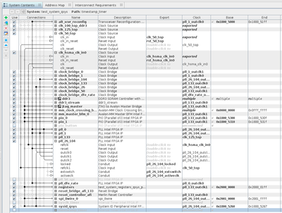
Can you show your connections in the System View tab and the component connections that are enabled with the options you've selected in the Block Symbol tab?
- Mark as New
- Bookmark
- Subscribe
- Mute
- Subscribe to RSS Feed
- Permalink
- Report Inappropriate Content
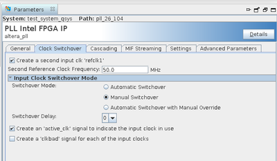
So are those two tabs in Quartus or Platform Designer? I see the "System Contents" and "Parameters" tabs in Platform Designer. They are showed below. If this isn't what you wanted please let me know:
The rest of the settings are defaults.
TomT...
- Mark as New
- Bookmark
- Subscribe
- Mute
- Subscribe to RSS Feed
- Permalink
- Report Inappropriate Content
Spitballing here. Since your two reference clocks are different, you may be running into the issue mentioned here about the second reference clock frequency (though I'm just noticing you mentioned matching the frequencies and running into the same issue): https://www.intel.com/content/www/us/en/docs/programmable/683359/17-0/ip-core-parameters-clock-switchover-tab.html
Have you considered using the clock control block instead? https://www.intel.com/content/dam/www/programmable/us/en/pdfs/literature/ug/ug_altclock.pdf
Sorry I was thinking of Pro. It's called System View there instead of System Contents. And you can access the Block Symbol tab from the View menu and then select a component to view all the component interfaces and individual signals.
- Mark as New
- Bookmark
- Subscribe
- Mute
- Subscribe to RSS Feed
- Permalink
- Report Inappropriate Content
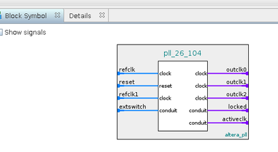
Here is the block view, Platform Designer believes it will have 2 clocks and the switch controls. But after Fitter, I look at the technology view and that isn't the case. Furthermore the signals extswitch and activeclk are on my QSYS generated interface but are not connected to this PLL like I expected. So Platform Designer is happy but Quartus Fitter is not happy.
Yes I did fudge it so both clocks had the same frequency into the tool and I got the same wrong result?
I do have the clock control block in the design for these two clocks, but I think you are saying I can have both clocks coming into one clock control block. Let me investigate more and get back to you.
TomT...
- Mark as New
- Bookmark
- Subscribe
- Mute
- Subscribe to RSS Feed
- Permalink
- Report Inappropriate Content
Are you saying that extswitch is just optimized away and not connected anywhere outside the system? You have it exported in Platform Designer so you have it connected to other logic or it's connected directly to an I/O pin. Are you saying that it's just gone from the design after compilation?
- Mark as New
- Bookmark
- Subscribe
- Mute
- Subscribe to RSS Feed
- Permalink
- Report Inappropriate Content
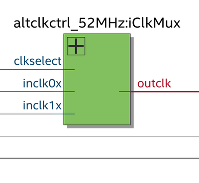
So this is the RTL view of the new ALTCLKCTRL block that I have put in. I made sure the two inclk pins only go to this block. clkselect is coming from a programmable register inside our Avalon Design so I know it is functional.
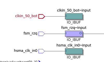
This is the MAPPED view, notice that the two clocks: clkin_50_bot and hsma_clk_in0 are now disconnected?
TomT...
- Mark as New
- Bookmark
- Subscribe
- Mute
- Subscribe to RSS Feed
- Permalink
- Report Inappropriate Content
Is your design complete and the clocks are connected to and clocking logic? If not, things will get optimized away like this.
- Mark as New
- Bookmark
- Subscribe
- Mute
- Subscribe to RSS Feed
- Permalink
- Report Inappropriate Content
sstrell, not a newbie. I have spent the day confirm the connectivity to ensure this wouldn't happen. I started by using the front it of the PLL to do the clock switching in manual mode. That didn't seem to be working which was my original post. It was suggested to put an ALTCLKCTRL in the path of the two clocks so only one clock was going to the PLL. That is move the clock switching from the PLL IP Block to outside of it. I added that component and reworked my top level logic to ensure it was correct and that the clocks from pins had no other loads (this was a problem that I resolved -- I have inherited this design and am attempting to make it better and more stable while also rolling in feature requests).
So I expect when I have properly connected up clocks to an ALTCLKCTRL block which then feeds a PLL that when we run FITTER that it doesn't disconnect everything between the ALTCLKCTRL block and the PLL? But that seems to be what I am showing and what happened.
I guess I will have to make a super small testcase to try this out on for everyone!
TomT...
- Mark as New
- Bookmark
- Subscribe
- Mute
- Subscribe to RSS Feed
- Permalink
- Report Inappropriate Content
Created a small testcase that seems to get past this disappearing logic problem, but it runs into the next problem in that I have two dedicated locations for these clocks: mentioned earlier AL5 and AP29. Apparently in this device: 5AGXFB3H4F35C4 it cannot route to the ALTCLKCNTL block because it cannot location a Global Clock Driver. I can provide the smaller reference design if necessary. But with this knowledge I am kind of stuck! I have two clocks on the Bottom of the die which have the following characteristics:
clkin_50_bot pin: AL5, CLK9p
hsma_clk_in pin: AP29, CLK3p
So can someone explain to my why I have two clocks on dedicated clock pins that cannot be routed? Here is the Fitter Error:
- Mark as New
- Bookmark
- Subscribe
- Mute
- Subscribe to RSS Feed
- Permalink
- Report Inappropriate Content
Do you have a bunch of clocks in your design? Maybe you are overusing the global routing channels. You could try taking non-critical clock domains off the global routing channels with the "Global Signal" assignment in the Assignment Editor set to No. Or perhaps at least overusing the GCLK networks that are fed by the particular clock in put pins listed here: https://www.intel.com/content/www/us/en/docs/programmable/683213/current/clock-input-pin-connections-to-gclk.html
For example, clk3p can only feed GCLK0-3 and clk9p can only feed GCLK8-11, so if you're already using those global routing channels, the Fitter wouldn't be able to make a connection (though the error message for clk9p indicates it tried looking at everything other than GCLK8-11; weird). This is why global signal management in the Assignment Editor may help.
Very strange problem. I don't know if I'm helping or just confusing matters.
- Mark as New
- Bookmark
- Subscribe
- Mute
- Subscribe to RSS Feed
- Permalink
- Report Inappropriate Content
The real design has lots of clocks, but this was happening on a design where there is the ALTCLKCTRL block and one PLL with all signals coming from the IO; that is it 2 IP blocks and connections. I need these PIN assignments as that is what I have access to on the Development Board; so they are not changing.
Let me package up the example and attach it to this case. It is so trivial it should work but I am baffled why the tool cannot do this. This might take me today to get approval to move this test design out of our secure area. Sorry don't have access to Quartus anywhere else for this project.
Thanks,
TomT...
- Tags:
- Fine
- Mark as New
- Bookmark
- Subscribe
- Mute
- Subscribe to RSS Feed
- Permalink
- Report Inappropriate Content
Here is the simple testcase which fails in FITTER as show above.
Any idea why this fails???
TomT...
- Mark as New
- Bookmark
- Subscribe
- Mute
- Subscribe to RSS Feed
- Permalink
- Report Inappropriate Content
Any thoughts on why this simple example doesn't compile?
TomT...
- Mark as New
- Bookmark
- Subscribe
- Mute
- Subscribe to RSS Feed
- Permalink
- Report Inappropriate Content
- Subscribe to RSS Feed
- Mark Topic as New
- Mark Topic as Read
- Float this Topic for Current User
- Bookmark
- Subscribe
- Printer Friendly Page
