- Mark as New
- Bookmark
- Subscribe
- Mute
- Subscribe to RSS Feed
- Permalink
- Report Inappropriate Content
Hi,
Here is my situation: I have created design which contains PLL with dynamic reconfiguration, and dynamic phase shift options.- Input clk of PLL can change in range from 5MHz to 200MHz.
- Each time input clock is changed PLL is reconfigured to work with new frequency and phase of PLL output clock is also changed to fine tune sampling on input data.
- PLL is instantiaded in design with initial parameters: inclk0= 200MHz, divide_by = 1, multiply_by = 1, clk0_phase_shift = 0.
Link Copied
8 Replies
- Mark as New
- Bookmark
- Subscribe
- Mute
- Subscribe to RSS Feed
- Permalink
- Report Inappropriate Content
Here is a part for PLL constrains of my initial sdc file:
create_clock -period 5 -name pll_inclk
create_generated_clock 	-name  pll_outclk_c0
					-source ]
					-phase 0 ]
So i have project compiled with my initial PLL constrains. What should i do next? Should i create separate sdc files for case in which i am interested just for timing analysis or i can say that if my design meets timing in max frequency it should be OK in lover frequencies?
- Mark as New
- Bookmark
- Subscribe
- Mute
- Subscribe to RSS Feed
- Permalink
- Report Inappropriate Content
What is the range of the OUTPUT clock of the PLL? That would be the clock to your logic, correct? If so, a 'fast' output clock .sdc should probably be sufficient (ie, whatever the highest output clock rate you plan to generate). As long as the FPGA can meet the fastest timing your clock will generate, it will be able to run at a slower rate (basically all the way to DC).
The phase shift on the output clock should not effect the timing of your logic at all. About the only critical issue (other than meeting timing) will be adding the appropriate input synchronizers to capture the input data reliably.- Mark as New
- Bookmark
- Subscribe
- Mute
- Subscribe to RSS Feed
- Permalink
- Report Inappropriate Content
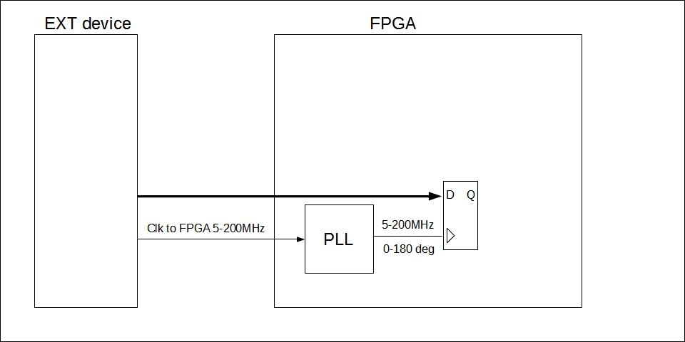
--- Quote Start --- What is the range of the OUTPUT clock of the PLL? --- Quote End --- Same as input 5 - 200MHz. --- Quote Start --- That would be the clock to your logic, correct? --- Quote End --- Not only for internal logic. Output clock of PLL is used as a latch clock for input data of external device. Here is basic drawing of my setup : https://alteraforum.com/forum/attachment.php?attachmentid=13494&stc=1 External device provides clock and data bus for FPGA device. Clock from external device can be changed in range 5-200MHz. Every time when clock from external device has changed FPGA PLL is also reconfigured to work with that frequency (PLL output clock is always the same as input clock) and phase setting is changed to find valid sampling window. --- Quote Start --- About the only critical issue (other than meeting timing) will be adding the appropriate input synchronizers to capture the input data reliably. --- Quote End --- That is the reason of this post. I am not concerned in meeting timing in FPGA internal logic , as you said max frequency constrain should be enough to see if it will work. I am interested in checking timing on input pins. For example: I have design compiled with my described initial parameters. Input clk to PLL is 200MHz, output clock from PLL is 200MHz, phase shift 0 deg. External device can be replaced with different one (different frequency or in some cases even different data delays on data bus). When different external device is connected I can reconfigure FPGA PLL and change phase to find valid window. Bu how to know from TimeQuest if those two devices will work?
- Mark as New
- Bookmark
- Subscribe
- Mute
- Subscribe to RSS Feed
- Permalink
- Report Inappropriate Content
Let me summarize my understanding of your problem:
- Your external device supplies a 5-200 MHz clock. - The delay from the external delay may also change. - You plan to deal with this by changing the PLL configuration, to have a suitable output frequency and phase. An interesting approach. A couple of questions to narrow down the problem: Q1: Do you have discrete set of frequencies/delays or are you in a situation where anything is possible? Q2: Is your entire design running on that single PLL output clock or do you have multiple clocks?- Mark as New
- Bookmark
- Subscribe
- Mute
- Subscribe to RSS Feed
- Permalink
- Report Inappropriate Content
--- Quote Start --- - Your external device supplies a 5-200 MHz clock. --- Quote End --- Yes --- Quote Start --- - The delay from the external delay may also change. --- Quote End --- Yes --- Quote Start --- - You plan to deal with this by changing the PLL configuration, to have a suitable output frequency and phase. --- Quote End --- Yes --- Quote Start --- An interesting approach. --- Quote End --- Why? Am I trying to solve this problem in some kind of unusual way? :) --- Quote Start --- Q1: Do you have discrete set of frequencies/delays or are you in a situation where anything is possible? --- Quote End --- Frequency can be any from the given range 5-200 MHz and 3 sets of delays (3 different external devices) --- Quote Start --- Q2: Is your entire design running on that single PLL output clock or do you have multiple clocks? --- Quote End --- There are more clocks and other interfaces but data is passed to other clock domain by using dual clock FIFO. Does this make any difference?
- Mark as New
- Bookmark
- Subscribe
- Mute
- Subscribe to RSS Feed
- Permalink
- Report Inappropriate Content
--- Quote Start --- Why? Am I trying to solve this problem in some kind of unusual way? --- Quote End --- In a word, yes. It seems to be more complicated than necessary. Can you characterize the timing of the input data with respect to the input clock, both as seen at the input pins to the FPGA? If for example the input data changes are referenced to the input clock rising edge then just sampling the input data on either the rising (or falling) edge of the clock might suffice. Using a PLL as you propose is probably possible, but it seems like overkill, and reconfiguring a PLL for such a wide locking/tracking range will not be straightforward. You will have to have frequency detection logic, and reprogram the PLL locking parameters based on the detected frequency.
- Mark as New
- Bookmark
- Subscribe
- Mute
- Subscribe to RSS Feed
- Permalink
- Report Inappropriate Content
--- Quote Start --- Can you characterize the timing of the input data with respect to the input clock, both as seen at the input pins to the FPGA? --- Quote End --- Here is basic drawing with ideal situation: https://www.alteraforum.com/forum/attachment.php?attachmentid=13507 Launch CLK - clock from external device Data delay - time after launch edge data becomes valid (delay is different for different external devices) Latch CLK - PLL output clock used for latching data. As you can see from diagram this is DDR interface so both (rising and falling edges are used). PLL is used to centre align latch clock with data and capture data in the middle of valid window. --- Quote Start --- Using a PLL as you propose is probably possible, but it seems like overkill, and reconfiguring a PLL for such a wide locking/tracking range will not be straightforward. --- Quote End --- I am not talking about just one PLL configuration. As I said before I have already implemented PLL with dynamic reconfiguration option and I can change PLL parameters such as M,N,C counter values, phase shift ect. while FPGA is operating. In this case there is no need to have wide PLL lock range. PLL lock range depends on PLL VCO frequency and M,N parameters. If frequency of external device is changed FPGA PLL gets new parameters (M,N,C counter values, phase shift ect.) and PLL reconfiguration is triggered.
- Mark as New
- Bookmark
- Subscribe
- Mute
- Subscribe to RSS Feed
- Permalink
- Report Inappropriate Content
Hi,
I had never came across such a solution. Then again, I never came across your exact problem. :) (1) If you're going to change the phase of one of the PLL outputs, I'll point out you'll need to consider that clock asynchronous to the rest. This means dual clock FIFO with 2+ states, etc. (2) AFAIK, TimeQuest does not support Multi-Mode analysis, which would be the ideal to analyze your solution Maybe it's possible to emulate it by creating multiple clock constraints at the input clock pin and adding input delays to each clock. Not sure if this will work. (3) Personally, this is how I'd do this: implement a solution which can deal with arbitrary input delays and otherwise simply constrain my design for 200 MHz. Given the data rates involved, I'd go for 4X synchronous oversampling of the input (see Xilinx xapp523 for inspiration). Another possibility would be to dynamically adjust the phase of the sampling clock produced by the PLL until I can reliably receive data.
Reply
Topic Options
- Subscribe to RSS Feed
- Mark Topic as New
- Mark Topic as Read
- Float this Topic for Current User
- Bookmark
- Subscribe
- Printer Friendly Page