- Mark as New
- Bookmark
- Subscribe
- Mute
- Subscribe to RSS Feed
- Permalink
- Report Inappropriate Content
Link Copied
- Mark as New
- Bookmark
- Subscribe
- Mute
- Subscribe to RSS Feed
- Permalink
- Report Inappropriate Content
Hi BSiri,
The hot socketing circuit does not include nSTATUS pin. This to ensure nSTATUS pin are able to operate during configuration (not in tri-states mode).
Thanks
- Mark as New
- Bookmark
- Subscribe
- Mute
- Subscribe to RSS Feed
- Permalink
- Report Inappropriate Content
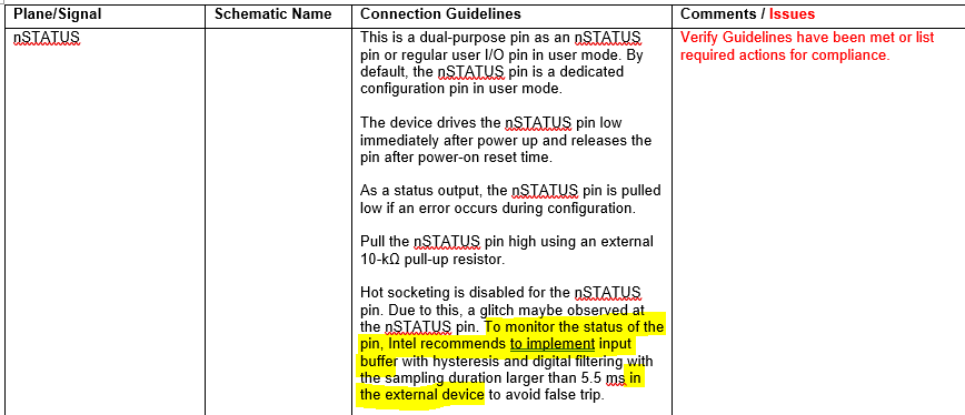
Thanks for your answer. I already knew that hot-socketing does not support nstatus and I found in the connection guideline that
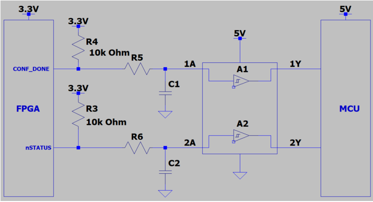
I have to implement an external input buffer. Is my schematic correct?
Thank you
- Mark as New
- Bookmark
- Subscribe
- Mute
- Subscribe to RSS Feed
- Permalink
- Report Inappropriate Content
Hi Bsiri,
You can use your schematic.
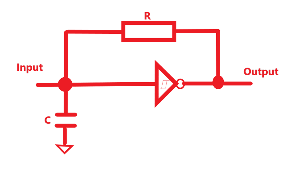
However, based on my recommendation, I suggest you to parallel the Resistor (R). Refer to picture below (sorry for my ugly drawing... 😂 😂):
1.When Input switched on the capacitor voltage is zero, thus the output is HIGH.
- The high output voltage will start to charge C via R.
- When the capacitor reach the higher threshold the inverter sees this as high voltage and the output will go LOW
2.When output is LOW:
- The capacitor will now start discharge to the low output through R.
- When the capacitor reach the lower threshold the inverter sees this as low voltage and the output will go HIGH.
3.The capacitor will start charge again and the whole thing repeats.
I hope this will help.
Thanks
- Subscribe to RSS Feed
- Mark Topic as New
- Mark Topic as Read
- Float this Topic for Current User
- Bookmark
- Subscribe
- Printer Friendly Page


