- Mark as New
- Bookmark
- Subscribe
- Mute
- Subscribe to RSS Feed
- Permalink
- Report Inappropriate Content
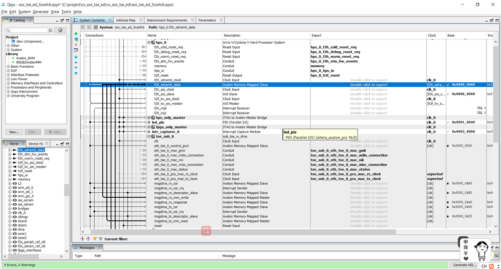
在使用hps调用tse ip核中,根据https://rocketboards.org/foswiki/Projects/AlteraSoCTripleSpeedEthernetDesignExample的tse示例工程。通过两个scatter-Gather DMA(master)与HPS中的f2h sdram(slave)进行tse的数据通信。
问题是:我如何通过上位机直接访问这个f2h sdram的内部数据,f2h sdram的寻址空间为0x00000000~0xffffffff,master为DMA,我不是很清楚是否能通过hps直接访问到sdram内部的数据(寻址空间是重复的),从而通过tse发送数据。

Link Copied
- Mark as New
- Bookmark
- Subscribe
- Mute
- Subscribe to RSS Feed
- Permalink
- Report Inappropriate Content
- Mark as New
- Bookmark
- Subscribe
- Mute
- Subscribe to RSS Feed
- Permalink
- Report Inappropriate Content
Hello:
as shown in the graphic,f2h SDRAM connects to the scatter-Gather DMA,scatter-Gather DMA is mater and SDRAM is slave ,how i can access SDRAM through hps directly .what is the direction between DMA and HPS,can I access through hps directly,or how i can access DMA? SDRAM address is 0x00000000~0xffffffff
- Mark as New
- Bookmark
- Subscribe
- Mute
- Subscribe to RSS Feed
- Permalink
- Report Inappropriate Content
Hello,
F2H SDRAM bridge is used to access DDR memory of HPS side by FPGA master (processor, DMA, or JTAG Master). You can read/write without any issues. the only thing that need to be considered is, the bridges should be enabled. To make this safely, let HPS configures the FPGA, and boots linux; on this case, you will guarantee the bridge enablement.
If you want to access DDR from HPS side, this can be done easily by using memtool in linux, you can read and write the DDR.
For DMA, you have to initialize the DMA to do the job for you. usually we use Nios II to configure the DMA, and then the DMA will transfer the data from FPGA side, to SDRAM HPS side. I am attaching an example of how to do that.
Thanks
- Mark as New
- Bookmark
- Subscribe
- Mute
- Subscribe to RSS Feed
- Permalink
- Report Inappropriate Content
- Mark as New
- Bookmark
- Subscribe
- Mute
- Subscribe to RSS Feed
- Permalink
- Report Inappropriate Content
Hello,
thanks for your reply,but i still don't clearly about the relationship between the DDR3 and the f2h SDRAM address.if i add 6 f2h SDRAMs.how can i Map the address relationships between them and the DDR3. every SDRAM address is 0x00000000~0xffffffff,what is the DDR3 address? for example ,i use DMA,should i control the DMA descriptor to access the DDR directly,and then access DDR through hps directly.I'm sorry it's my first time use tse and scatter-Gather DMA ip core.i referred the design downloaded in
https://rocketboards.org/foswiki/Projects/AlteraSoCTripleSpeedEthernetDesignExample?rpm_id=8083970&erpm_id=8083970&erpm_id=8083970&erpm_id=8083970&erpm_id=8083970&erpm_id=8083970&erpm_id=8083970&erpm_id=8083970&erpm_id=8083970&_ga=2.113202945.401678115.1550048297-1001826037.1545013780&erpm_id=8083970l
- Mark as New
- Bookmark
- Subscribe
- Mute
- Subscribe to RSS Feed
- Permalink
- Report Inappropriate Content
Hello,
This is done through the SDRAM controller subsystem. each controller is connected to a DDR. Only one f2sdram bridge is sufficient.
As shown in the design I sent to you earlier. you can connect Avalon master on FPGA to Address Span extender IP. Inside this IP, you can define the starting region of your SDRAM which assigned to FPGA. This is configurable option.
in the example above, the address span extender looks at this sdram with base address of 0x20000000, so anything below this address is not seen by FPGA.
Thanks
- Mark as New
- Bookmark
- Subscribe
- Mute
- Subscribe to RSS Feed
- Permalink
- Report Inappropriate Content
- Mark as New
- Bookmark
- Subscribe
- Mute
- Subscribe to RSS Feed
- Permalink
- Report Inappropriate Content
- Mark as New
- Bookmark
- Subscribe
- Mute
- Subscribe to RSS Feed
- Permalink
- Report Inappropriate Content
- Subscribe to RSS Feed
- Mark Topic as New
- Mark Topic as Read
- Float this Topic for Current User
- Bookmark
- Subscribe
- Printer Friendly Page