- 新着としてマーク
- ブックマーク
- 購読
- ミュート
- RSS フィードを購読する
- ハイライト
- 印刷
- 不適切なコンテンツを報告
Hey folks,
Here is the pinout diagram for the Altera USB-Blaster JTAG cable as well as the USB box IDC socket. http://www.digital-circuitry.com/IMAGES/webpage/MyLAB/Thumb/Altera_USB-Blaster_JTAG_pinout.jpg hi-res copy (1200 x 645 pixels): http://www.digital-circuitry.com/images/webpage/mylab/altera_usb-blaster_jtag_pinout.jpg (http://www.digital-circuitry.com/images/webpage/mylab/altera_usb-blaster_jtag_pinout.jpg) Regards, -Gerry http://www.digital-circuitry.com/index.htm (http://www.digital-circuitry.com/index.htm)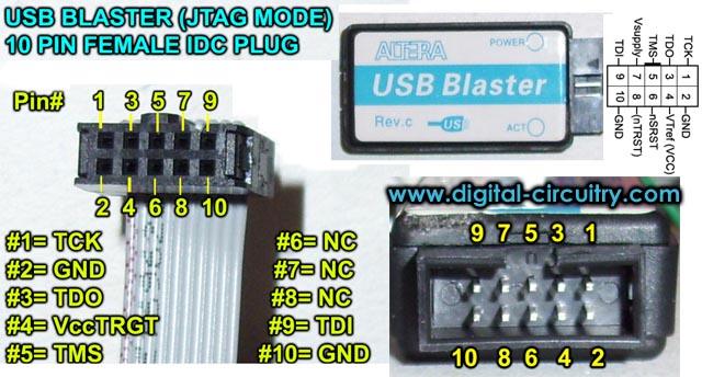
コピーされたリンク
1 返信
- 新着としてマーク
- ブックマーク
- 購読
- ミュート
- RSS フィードを購読する
- ハイライト
- 印刷
- 不適切なコンテンツを報告
And in the user manual (http://www.altera.com/literature/ug/ug_usb_blstr.pdf) on page 2-4 you also have the pinout for the (less used) AS and PS modes.