- Mark as New
- Bookmark
- Subscribe
- Mute
- Subscribe to RSS Feed
- Permalink
- Report Inappropriate Content
Hi: This is my first design using CPLD. Can someone comment on my layout before I tell the board house to run it?
I'm using an EPM7064STC44-10 Specifically, is my ISP connector correct, do I need pull ups or pull downs, etc. Enough bypass caps? Also, I'm getting the clock from the uP's ECLK output, which is 4MHz. I added pads for a cap to slow the edges if necessary. The heavy green line is a potting shell, so I buffered the 24 I/O signals on the outside of the potting shell. The buffers can be replaced if stuff happens. Thanks for looking. http://www.jandssafeguard.com/layout.png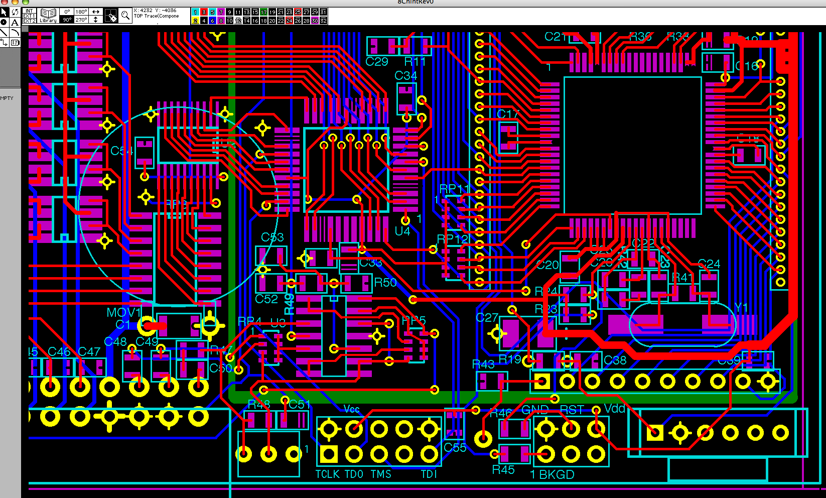
Link Copied
4 Replies
- Mark as New
- Bookmark
- Subscribe
- Mute
- Subscribe to RSS Feed
- Permalink
- Report Inappropriate Content
Hello,
I understand, that you have a two layer PCB with GND flooded top layer. Cause GND display is disabled, I can't see how this net is actual connected. Obviously GND connection can't be optimal, the same with supply bypass, but I wouldn't expect particular problems for the CPLD in this design. There may be a danger of double counts and timing violations with a ringing clock, but the said capacitor could help in this case. TCK should have a pulldown (e. g. 10K), TDI and TMS may have pullups. Regards, Frank- Mark as New
- Bookmark
- Subscribe
- Mute
- Subscribe to RSS Feed
- Permalink
- Report Inappropriate Content
Thanks
Found a missing ground. Updating artwork... Adding pads for TCLK pulldown and TDI and TDS pullups. So, do I only need to install the pullups if the device won't program? I have 150 ohm series resistors (R45 and R46) for protection on the programming pins to the 9S12 uP. Good idea or bad idea on the Altera? As Don Lancaster says "protect the protection." New artwork: http://www.jandssafeguard.com/topside.jpg http://www.jandssafeguard.com/solderside.jpg
- Mark as New
- Bookmark
- Subscribe
- Mute
- Subscribe to RSS Feed
- Permalink
- Report Inappropriate Content
Hello,
displaying the flooded bottom layer, the ground connetion looks much better now. Regarding the pullups, the devicé would usually programm without them. Altera USB Blaster has e. g. 100k TCK pulldown, 100k TMS pullup and no TDI pullup. Possible issue is succeptibility to coupled switching noise, that may cause erroneous JTAG circuit behaviour. Thus the suitable resistance value depends on strength of interfering signals. If there isn't plenty of room for additional parts, I would provide a TCK pulldown as minimal means. Pullups at the other pins could possibly slightly reduce supply current. Regards, Frank- Mark as New
- Bookmark
- Subscribe
- Mute
- Subscribe to RSS Feed
- Permalink
- Report Inappropriate Content
Frank:
I added the pads for three resistors as you advised. Thanks again for your fine help. John Pizzuto J&S Electronics
Reply
Topic Options
- Subscribe to RSS Feed
- Mark Topic as New
- Mark Topic as Read
- Float this Topic for Current User
- Bookmark
- Subscribe
- Printer Friendly Page