- Mark as New
- Bookmark
- Subscribe
- Mute
- Subscribe to RSS Feed
- Permalink
- Report Inappropriate Content
Hi,
What is the correct way to constrains source synchronous inputs in this case:External device provides clock with data. External device launches data on falling edge. FPGA latches data on rising edge. I asume that in this case data comes to FPGA center aligned so I created constraints:#Base clock
create_clock -period "100MHz" -name CLK_IN -waveform {5 10}# Virtual clock
create_clock -name CLK_IN_VIRT -period "100MHz"
set_input_delay -clock -max $in_max_value
set_input_delay -clock -min $in_min_value
I have atached TimeQuest waveform. http://www.alteraforum.com/forum/attachment.php?attachmentid=12716&stc=1 Do I have to add some exceptions to represent correct clock relationship, because with my constraints TimeQuest does not show that data is launched by falling clock edge? Thanks
Link Copied
10 Replies
- Mark as New
- Bookmark
- Subscribe
- Mute
- Subscribe to RSS Feed
- Permalink
- Report Inappropriate Content
Hello,
By using following, Timequest will consider that data is launched by falling edge. # Base clock create_clock -period "100MHz" -name CLK_IN [get_ports CLK_IN] # Virtual clock create_clock -name CLK_IN_VIRT -period "100MHz" set_input_delay -clock [get_clocks CLK_IN_VIRT ] -clock_fall -max $in_max_value [get_ports {DATA*}] set_input_delay -clock [get_clocks CLK_IN_VIRT ] -clock_fall -min $in_min_value [get_ports {DATA*}] changes compared to your constraints: I have removed -waveform option in create_clock for CLK_IN and have added -clock_fall in set_input_delay. i am not sure how should your design be properly constrained. Hence I would not be able to provide to the point answer. Sorry. There is one Application note (AN433 -Constraining and Analyzing Source-Synchronous Interfaces ). Just search on google and you will find it. It may be helpful. one question : Which clock have you been using to capture data? Are you using clock directly coming into FPGA? Thank you, Bhaumik- Mark as New
- Bookmark
- Subscribe
- Mute
- Subscribe to RSS Feed
- Permalink
- Report Inappropriate Content
Hi,
Thank you Bhaumik. --- Quote Start --- one question : Which clock have you been using to capture data? Are you using clock directly coming into FPGA? --- Quote End --- I am using CLK_IN which directly comes to FPGA, PLL is not used.- Mark as New
- Bookmark
- Subscribe
- Mute
- Subscribe to RSS Feed
- Permalink
- Report Inappropriate Content
Hello,
Here is what I would do if I am there. (1) I would take one pll with following parameters: -> Mode : Source synchronous mode ( https://www.altera.com/support/support-resources/operation-and-testing/pll-and-clock-management/pll-glossary.html#source_synchronous_mode ) -> Input clock : Clock which is coming from external device -> Output clock 0 : With same frequency as input clock (2) Then I would use pll's output clock 0 to sample incoming signals. My SDC file would have following constraints : # Base clock create_clock -period "100MHz" -name CLK_IN [get_ports CLK_IN] # Virtual clock create_clock -name CLK_IN_VIRT -period "100MHz" # Deriving PLL clocks derive_pll_clocks # Derive clock uncertainty derive_clock_uncertainty set_input_delay -clock [get_clocks CLK_IN_VIRT ] -clock_fall -max $in_max_value [get_ports {DATA*}] set_input_delay -clock [get_clocks CLK_IN_VIRT ] -clock_fall -min $in_min_value [get_ports {DATA*}] I have assumed here that incoming clock is continuous. is this correct? I am learning these timing constraints. So, feel free to share your opinion if you have any concern. Thank you, Bhaumik- Mark as New
- Bookmark
- Subscribe
- Mute
- Subscribe to RSS Feed
- Permalink
- Report Inappropriate Content
Hi,
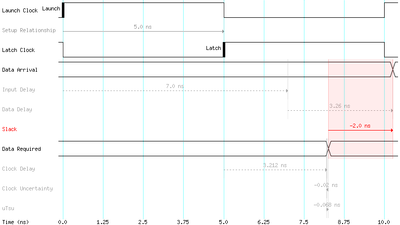
thank you for your response, Bhaumik. --- Quote Start --- Here is what I would do if I am there. (1) I would take one pll with following parameters: -> Mode : Source synchronous mode ( https://www.altera.com/support/support-resources/operation-and-testing/pll-and-clock-management/pll-glossary.html#source_synchronous_mode ) -> Input clock : Clock which is coming from external device -> Output clock 0 : With same frequency as input clock (2) Then I would use pll's output clock 0 to sample incoming signals. --- Quote End --- In my design there are no free PLL left, so I can not use it. --- Quote Start --- I have assumed here that incoming clock is continuous. Is this correct? --- Quote End --- Yes, clock is continous. I have corrected my timing constrainst by your previos post. Interface works correctly and clock relationchip seems to be correct but TimeQuest shows me that timing requirements ar not met. What could be done to achieve timing requrements? Here is updated waveform:http://www.alteraforum.com/forum/attachment.php?attachmentid=12722&stc=1 For input delay I am using tCO value from external device tCOmax=7ns, tCOmin is not specified so i have entered tCOmin=0. For input delay values i am using tco and tco min method from AN433 pdf. input maximum delay value = maximum trace delay for data + tco of external device – minimum trace delay for clockinput minimum delay value = min trace delay for data + tco min of external device – max trace delay for clock For now i have excluded trace delays from formulas. So my .sdc file looks like:
# Base clock
create_clock -period "100MHz" -name CLK_IN # Virtual clock
create_clock -name CLK_IN_VIRT -period "100MHz"
# parameters of external device
set tCO_max     7
set tCO_min     0
set in_max_value
set in_min_value
set_input_delay -clock  -clock_fall -max $in_max_value
set_input_delay -clock  -clock_fall -min $in_min_value
- Mark as New
- Bookmark
- Subscribe
- Mute
- Subscribe to RSS Feed
- Permalink
- Report Inappropriate Content
Hello,
Sorry for taking time to respond. Here are my thoughts: (1) Our clock period is 10ns and Tco (Max) is 7. This seems large value to me. It may be worth to re-check this value. (2) Minimum Tco you have considered is 0. Can we take some larger value? You may like to ask to manufacturer of external device. It would relax some timing requirements. (3) It seems that external device launches data only on negative edge. Is this correct? (4) One thing which we can do is to use Multicycle path between virtual clock and sampling clock. So that, instead of trying to capture data on next postive clock cycle, let ask it to capture data on second next positive edge. You need to add following constraints in your SDC file: set_multicycle_path -setup -from [get_clocks CLK_IN_VIRT ] -to [get_clocks CLK_IN] 2 No need to provide multi-cycle for hold. It will automatically take based on above command. BUT, in this case, I afraid we will violate hold timings. Thank you, Bhaumik- Mark as New
- Bookmark
- Subscribe
- Mute
- Subscribe to RSS Feed
- Permalink
- Report Inappropriate Content
Hi,
Thanks for you response. --- Quote Start --- (1) Our clock period is 10ns and Tco (Max) is 7. This seems large value to me. It may be worth to re-check this value. --- Quote End --- Here is timing parameters from external device http://www.cypress.com/file/136056/download (http://www.cypress.com/file/136056/download), page 9, table 3. Can you look at this paper, maybe I have missunderstood something? --- Quote Start --- (2) Minimum Tco you have considered is 0. Can we take some larger value? You may like to ask to manufacturer of external device. It would relax some timing requirements. --- Quote End --- What value do you suggest? I will try to write to support of external device to ask for those values. --- Quote Start --- (3) It seems that external device launches data only on negative edge. Is this correct? --- Quote End --- No, launch edge of external device can be configured to positive or negative edge. I have configured external device to launch data on negative edge thinking that data will come to FPGA center alligned. --- Quote Start --- (4) One thing which we can do is to use Multicycle path between virtual clock and sampling clock. So that, instead of trying to capture data on next postive clock cycle, let ask it to capture data on second next positive edge. You need to add following constraints in your SDC file: set_multicycle_path -setup -from [get_clocks CLK_IN_VIRT ] -to [get_clocks CLK_IN] 2 No need to provide multi-cycle for hold. It will automatically take based on above command. BUT, in this case, I afraid we will violate hold timings. --- Quote End --- I have added set_multicycle_path for setup and setup violation is gone but hold time violation had increased even more. But then I added same set_multicycle_path for hold: set_multicycle_path -hold -from [get_clocks CLK_IN_VIRT ] -to [get_clocks CLK_IN] 2 Now TimeQuest shows me that timing requirements are met. Here is setup: https://www.alteraforum.com/forum/attachment.php?attachmentid=12726 And for hold: https://www.alteraforum.com/forum/attachment.php?attachmentid=12727 Now I am a bit confused, can you explain set_multicycle_path cammand a bit more to me? Do we actualy making FPGA to capture data with next rising edge of clock with this command or this is only for timing analysis? I was thinking that set_multicycle_path cammand is useful when data changes in different rate than clock? Thanks.- Mark as New
- Bookmark
- Subscribe
- Mute
- Subscribe to RSS Feed
- Permalink
- Report Inappropriate Content
For input data to fpga, timequest needs to know data offset relative to its sampling clock edge. Thus what matters is getting the offset information right. You can either enter offset directly relative to falling edge as you did or modify it relative to latch edge at fpga pin.
Regarding multicycle path you are free to do that if needed at io but not internally. Inside fpga you can only apply it if indeed you are sampling any data after 1 or so clocks. For io this does not matter since as long as data stream is sampled correctly then it doesn't matter if there is delay of sampling. but io mulicycle does not relax timing on both tSU and tH, rather it relaxes on one member of this pair. Both still need not be violated. Internal multicycle that are result of slow data can relax timing on both. So in short it may not be needed in your case as it is a straight forward input case. Incidentally, in theory any internal design can also be applied multicycle style as io but then it requires substantial and weird change of code to account for delay...in such cases both min and max delay must be accomplished so that tSU and tH are not violated.- Mark as New
- Bookmark
- Subscribe
- Mute
- Subscribe to RSS Feed
- Permalink
- Report Inappropriate Content
Hi,
Thanks for reply kaz. So as I understand you are saying that multicycle is not needed in my case, since data is sampled at same clock period? What do you mean by saying: --- Quote Start --- You can either enter offset directly relative to falling edge as you did or modify it relative to latch edge at fpga pin --- Quote End --- . How it can be modified? So what to do next? Clock relationship seems to be correct by looking at TimeQuest waveform, but timing requirements are not met. Am I using tCO values for max/min delays in a wrong way or am I missing something else? Thanks- Mark as New
- Bookmark
- Subscribe
- Mute
- Subscribe to RSS Feed
- Permalink
- Report Inappropriate Content
--- Quote Start --- Hi, Thanks for reply kaz. So as I understand you are saying that multicycle is not needed in my case, since data is sampled at same clock period? What do you mean by saying: . How it can be modified? --- Quote End --- if your tCO is 7 ns relative to falling edge and clk period is 20 ns then it means it is 3ns from next rising edge --- Quote Start --- So what to do next? Clock relationship seems to be correct by looking at TimeQuest waveform, but timing requirements are not met. Am I using tCO values for max/min delays in a wrong way or am I missing something else? Thanks --- Quote End --- tCO min of 0 and tCO max of 7 gives 7 ns window of transition. This is a bit wide. I suspect tCO min to be closer to 7 than zero.
- Mark as New
- Bookmark
- Subscribe
- Mute
- Subscribe to RSS Feed
- Permalink
- Report Inappropriate Content
@ Kaz,
As usual, thank you for your helpful nature and sharing your inputs. :) @ vlrean, Here are my suggestions: (1) Cypress provides one example for using their chip with Altera device. ( I came to know from pdf which you shared in last link.) It would be good idea to see SDC file being used in that example. (2) --- Quote Start --- No, launch edge of external device can be configured to positive or negative edge. I have configured external device to launch data on negative edge thinking that data will come to FPGA center alligned. --- Quote End --- Please use positive edge of clock. In this way, there will be gap of 10ns between launch clock and latch clock. After configuring your device to launch data on positive edge, you need to modify your input delay constraints (Just need to remove -clock_fall.). So, now your SDC should look like : # Base clock create_clock -period "100MHz" -name CLK_IN [get_ports CLK_IN] # Virtual clock create_clock -name CLK_IN_VIRT -period "100MHz" # parameters of external device set tCO_max 7 set tCO_min 0 set in_max_value [expr $tCO_max] set in_min_value [expr $tCO_min] set_input_delay -clock [get_clocks CLK_IN_VIRT ] -max $in_max_value [get_ports {DATA*}] set_input_delay -clock [get_clocks CLK_IN_VIRT ] -min $in_min_value [get_ports {DATA*}] This should give us better (in your case, I should say best so far ) timing margin. (3) If both of above do not help, then you should contact Cypress saying you are running your clock on 100 MHz. In this case, what value you should consider for Tco(max) and Tco (min). (4) Regarding Multicycle explanation, download TimeQuest User Guide by Ryan Scoville from following location: http://www.alterawiki.com/wiki/timequest_user_guide. It contains good description about Multicycle path (Page 55 ) as well as other timing constraints. In your case, previously, we applied multicycle path to 'shift the window'. But now, as you are going to use positive edge, this is not required. Please remove multi-cycle path related constraints from your SDC file. Thank you for reading this big post.:) Kind Regards, Bhaumik
Reply
Topic Options
- Subscribe to RSS Feed
- Mark Topic as New
- Mark Topic as Read
- Float this Topic for Current User
- Bookmark
- Subscribe
- Printer Friendly Page