- Mark as New
- Bookmark
- Subscribe
- Mute
- Subscribe to RSS Feed
- Permalink
- Report Inappropriate Content
Hello all!
I'm trying to understand how to constrain source synchronous interfaces and I'm having some difficulties. Could someone please explain the following: When we have two flip flops inside the FPGA, the setup time on that path is equal to the clock period, i.e. the first flip flop launches data at 0ns, and the other should latch it at 10ns for a 100 MHz clock. In case of a single data rate source synchronous interface, when FPGA is the receiver and the transmitter is sending edge-aligned data, why is the launch edge equal to the latch edge? Why can't the transmitting flip flop send the data at 0ns, and FPGA capture it at 10 ns as in the case of an internal FPGA path? Why do those two paths (path inside FPGA, path from tx to fpga input) have different default setup/hold relationships? Please see the below image for the default setup/hold relationship of the edge aligned source synchronous interface which I'm having difficulty understanding. https://alteraforum.com/forum/attachment.php?attachmentid=14580&stc=1 Thank you!
Link Copied
- Mark as New
- Bookmark
- Subscribe
- Mute
- Subscribe to RSS Feed
- Permalink
- Report Inappropriate Content
--- Quote Start --- Hello all! When we have two flip flops inside the FPGA, the setup time on that path is equal to the clock period, i.e. the first flip flop launches data at 0ns, and the other should latch it at 10ns for a 100 MHz clock. --- Quote End --- No the setup relationship(not tSU) is 10ns, hold relationship is 0ns. The launch and latch must occur within the 10 ns window minus tSU+tH --- Quote Start --- In case of a single data rate source synchronous interface, when FPGA is the receiver and the transmitter is sending edge-aligned data, why is the launch edge equal to the latch edge? Why can't the transmitting flip flop send the data at 0ns, and FPGA capture it at 10 ns as in the case of an internal FPGA path? Why do those two paths (path inside FPGA, path from tx to fpga input) have different default setup/hold relationships? Please see the below image for the default setup/hold relationship of the edge aligned source synchronous interface which I'm having difficulty understanding. --- Quote End --- Launch is always first then data is latched on next clock. Who says otherwise?
- Mark as New
- Bookmark
- Subscribe
- Mute
- Subscribe to RSS Feed
- Permalink
- Report Inappropriate Content
--- Quote Start --- Launch is always first then data is latched on next clock. Who says otherwise? --- Quote End --- Ok, but why is then setup relationship=0ns at the FPGA input?
- Mark as New
- Bookmark
- Subscribe
- Mute
- Subscribe to RSS Feed
- Permalink
- Report Inappropriate Content
--- Quote Start --- Ok, but why is then setup relationship=0ns at the FPGA input? --- Quote End --- At the FPGA io you can play some games to achieve timing. option 1: usual default behavior i.e. latch on next edge option 2: same edge launch/latch; if that helps timing No 2 is possible because as long as data stream is sampled correctly it doesn't matter if delay or advance is introduced. In this case the fitter will see if it is achievable or not.
- Mark as New
- Bookmark
- Subscribe
- Mute
- Subscribe to RSS Feed
- Permalink
- Report Inappropriate Content
Inside fpga's rtl chain the default is strict that latch is on next edge. At io you the user have other choices. Remember the clk edge is arbitrary and what matters is sampling correctly rather specifically on a given clock edge.
- Mark as New
- Bookmark
- Subscribe
- Mute
- Subscribe to RSS Feed
- Permalink
- Report Inappropriate Content
--- Quote Start --- Launch is always first then data is latched on next clock. Who says otherwise? --- Quote End --- Just wanted to bring to your attention that Altera's documentation says otherwise. Screenshot from AN433, page 4: https://alteraforum.com/forum/attachment.php?attachmentid=14590&stc=1
- Mark as New
- Bookmark
- Subscribe
- Mute
- Subscribe to RSS Feed
- Permalink
- Report Inappropriate Content
Ok, thank you for you reply.
I saw in the Altera's source synchronous interface online training the default setup relationship at 0 ns (screenshot in my original post, blue arrow is setup), so I was wandering why this was the case.- Mark as New
- Bookmark
- Subscribe
- Mute
- Subscribe to RSS Feed
- Permalink
- Report Inappropriate Content
It says "may be"
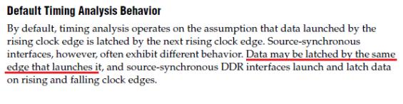
"By default, timing analysis operates on the assumption that data launched by the rising clock edge is latched by the next rising clock edge. Source-synchronous interfaces, however, often exhibit different behavior. Data may be latched by the same edge that launches it, and source-synchronous DDR interfaces launch and latch data on rising and falling clock edges"- Mark as New
- Bookmark
- Subscribe
- Mute
- Subscribe to RSS Feed
- Permalink
- Report Inappropriate Content
The receiver in an edge-aligned, source synchronous interface is responsible for phase shifting (180 degrees for SDR, 90 degrees for DDR) the incoming clock to center align it with the incoming data. TimeQuest for I/O interfaces works from the edge (the I/O) of the device. As such, in the edge-aligned case, the launch and latch edges are basically on top of each other. The FPGA with a PLL will shift the latch edge later to align it with the data.
So in the diagram you posted, picture the destination clock shifted 180 degrees to the right, keeping the red and blue arrows pointing to the same edges.- Subscribe to RSS Feed
- Mark Topic as New
- Mark Topic as Read
- Float this Topic for Current User
- Bookmark
- Subscribe
- Printer Friendly Page