Hi,
I plan to use Cyclone V with ADC LTC2387-18 (15 Msps, 18 bit).
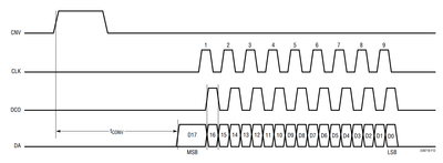
Timing diagram of ADC’s digital interface is shown below.
CNV and CLK are generated from FPGA (CNV is planned to be latched externally on the board using D-trigger in order to reduce jitter), and DCO and data (DA) are sent from the ADC.
What I want is to use IP core in order to exploit dedicated resources and latch data correctly, for example SERDES – ALTLVDS_RX core. But there is an issue - DCO signal has interruptions, it doesn’t switch permanently, that means we can't use ALTLVDS_RX core as I understand, because PLL could lose lock, and lock time is very uncertain – up to 1 ms according to Cyclone V datasheet. As I understand, we can’t use ALTLVDS_RX without PLL, just clocking dedicated SERDES directly from DCO.
In that case we need to use internal FPGA resources – registers from LEs, I suppose. It is a bit strange if it is so. But maybe somebody had experience with such types of ADCs and can help me. Maybe there are ways for using SERDES with such DCO signal or another IP cores.
Thanks!
Vadim
Hi Vadim
I hope I understand your situation correctly.
Yes, the ALTLVDS_RX is tied with a PLL. If your design has limitation towards the PLL lock time on the spec, then you have to create logics to implement the receiver.
Unfortunately we don't have sample reference design for this logic creation. For recommendation, we can make use of shift register and parallel register to construct the LVDS receiver.
We shall always refer to "Design Guidelines" mentioned in the doc below:
https://www.intel.com/content/dam/www/programmable/us/en/pdfs/literature/hb/cyc/cyc_c51009.pdf
Thanks.
Eng Wei
链接已复制
Thanks Vadim for your inquiry. Allow me some time to go through your design question and get back to you.
Thanks.
Eng Wei
Hi Vadim
I hope I understand your situation correctly.
Yes, the ALTLVDS_RX is tied with a PLL. If your design has limitation towards the PLL lock time on the spec, then you have to create logics to implement the receiver.
Unfortunately we don't have sample reference design for this logic creation. For recommendation, we can make use of shift register and parallel register to construct the LVDS receiver.
We shall always refer to "Design Guidelines" mentioned in the doc below:
https://www.intel.com/content/dam/www/programmable/us/en/pdfs/literature/hb/cyc/cyc_c51009.pdf
Thanks.
Eng Wei
Hi all!
Well, in case the PLL is tied with ALTLVDS_RX core, I suppose that maybe we could use pfdena signal for locking the DCO and so on, but in general we should create receiver logic from LEs.
----
Ivan
Hi Vadim
I’m glad that your question has been addressed, I now transition this thread to community support. If you have a new question, feel free to open a new thread to get the support from Intel experts. Otherwise, the community users will continue to help you on this thread. Thank you.
Eng Wei
