- Mark as New
- Bookmark
- Subscribe
- Mute
- Subscribe to RSS Feed
- Permalink
- Report Inappropriate Content
good evening !
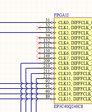
background: i am now trying to design a new develop FPGA( CYCLONE 3 EP3C40Q240C8) board. it has 2 ADC chips(ADS 5272http://www.ti.com/lit/ds/symlink/ads5272.pdf) which owns 16 channels of differential LVDS outputs totally. i want to connect the 16 channels(32 pins) to the FPGA. so my problems: i know Alteradevices have dedicated LVDS transmitters and receivers containing serializer ordeserializer hard-IP blocks. but i can only find 14 channls for the LVDS differential input except these used for clocks(as showed in Picture below). http://www.alteraforum.com/forum/attachment.php?attachmentid=10630&stc=1 so , 1. is it possible to use the I/O pins as the LVDS differential inpus? 2. can i use some channels from Clock part?
Link Copied
3 Replies
- Mark as New
- Bookmark
- Subscribe
- Mute
- Subscribe to RSS Feed
- Permalink
- Report Inappropriate Content
Hi,
Those seems more like dedicated clock pins. There should be some differential pins named DIFFIO_T/RXX. However I am not sure about that symbol in the schematics. If you cannot find in the symbol, you can try to cross check with the pin out file of the device to find the specific pins that are differential pins.- Mark as New
- Bookmark
- Subscribe
- Mute
- Subscribe to RSS Feed
- Permalink
- Report Inappropriate Content
Answering your questions:
1. is it possible to use the I/O pins as the LVDS differential inpus? - I believe you are referring to using single ended IO pin as differential input. Ideally you could do that by inverting the input signal to one of the input pin to make up p and n pair. However, you should expect skew between the p and n legs since you have a inversion in place. The dedicated LVDS input is design to ensure minimal skew between p and n legs. 2. can i use some channels from Clock part? - Generally the dedicated clock input pins will have dedicated routing to clock network. Not sure if Quartus II will allow you to use as normal input. You could did a quick try by running Quartus II compilation.- Mark as New
- Bookmark
- Subscribe
- Mute
- Subscribe to RSS Feed
- Permalink
- Report Inappropriate Content
There is plenty of LVDS I/O to allow you to interface that ADC to your chosen Cyclone III.
I recommend you connect the ADCLK and LCLK LVDS pairs to dedicated clock input pins. These dedicated clock input pins can be configured for LVDS operation and, as someone has already pointed out, feed directly onto clock networks internally. They can also feed PLLs if required. They offer good flexibility in that respect. The other 8 OUTx p/n pairs can just feed 'ordinary' I/O. Refer to the pin information for the cyclone® iii ep3c40 device (https://www.altera.com/content/dam/altera-www/global/en_us/pdfs/literature/dp/cyclone3/ep3c40.pdf) spreadsheet for that part. The 'Optional Funtion(s)' column identifies all he I/O that can be used as an LVDS pair. All the 'DIFFIO_xx' are suitable - plenty to chose from. Similarly, 'DIFFCLK_xx' are suitable dedicated clock input pairs. Make sure you connect all these signals, including the clocks, to banks powered at 2.5V. Regards, Alex
Reply
Topic Options
- Subscribe to RSS Feed
- Mark Topic as New
- Mark Topic as Read
- Float this Topic for Current User
- Bookmark
- Subscribe
- Printer Friendly Page