- Mark as New
- Bookmark
- Subscribe
- Mute
- Subscribe to RSS Feed
- Permalink
- Report Inappropriate Content
Hey All,
I have an interesting issue. I have a EP2C35F484 FPGA mounted on a FireflyII board (adds some memory, an oscillator, serial configuration chip and max232 converter). I am able to load a NiosII core onto the FPGA and run a simple counter but when I try to do anything in VHDL, even the simplest core does not seem to run. For instance, (using the schematic design mode) I simply connect an input to an output, assign the clock to the input pin and then assign the output to a physical pin on my board. As I understand it, I should see the clock being output to the physical pin, yes? I'm using the JTAG usb blaster to load the core, not worrying about the serial configuration chip yet. This seems like a very simple task but its really getting me stuck, especially because the NiosII core seems to work just fine. Any suggestions?Link Copied
- Mark as New
- Bookmark
- Subscribe
- Mute
- Subscribe to RSS Feed
- Permalink
- Report Inappropriate Content
Check whether you had a legal FPGA pin-out for your board for the Quartus compile with your VHDL.
- Mark as New
- Bookmark
- Subscribe
- Mute
- Subscribe to RSS Feed
- Permalink
- Report Inappropriate Content
The output pin was a valid pin. I used the same output pin in the NIOS application wihtout any problem.
- Mark as New
- Bookmark
- Subscribe
- Mute
- Subscribe to RSS Feed
- Permalink
- Report Inappropriate Content
--- Quote Start --- The output pin was a valid pin. I used the same output pin in the NIOS application wihtout any problem. --- Quote End --- It doesn't make sense to say your vhdl doesn't work while nios works(nios is just vhdl platform produced by SOPC). I am sure your testing is wrong, try signaltap instead of pins and make sure your vhdl is not optimised away.
- Mark as New
- Bookmark
- Subscribe
- Mute
- Subscribe to RSS Feed
- Permalink
- Report Inappropriate Content
--- Quote Start --- Hey All, I have an interesting issue. I have a EP2C35F484 FPGA mounted on a FireflyII board (adds some memory, an oscillator, serial configuration chip and max232 converter). I am able to load a NiosII core onto the FPGA and run a simple counter but when I try to do anything in VHDL, even the simplest core does not seem to run. For instance, (using the schematic design mode) I simply connect an input to an output, assign the clock to the input pin and then assign the output to a physical pin on my board. As I understand it, I should see the clock being output to the physical pin, yes? I'm using the JTAG usb blaster to load the core, not worrying about the serial configuration chip yet. This seems like a very simple task but its really getting me stuck, especially because the NiosII core seems to work just fine. Any suggestions? --- Quote End --- Hi, how did you add your schematic to your Nios System ? Kind regards GPK
- Mark as New
- Bookmark
- Subscribe
- Mute
- Subscribe to RSS Feed
- Permalink
- Report Inappropriate Content
I'm using one of the example applications that come with the NIOS design suite: http://www.altera.com/support/examples/nios2/exm-hello_free.html. The design was already inserted into a schematic. All I had to do was assign the LED output pins. This simple counter example works and I am able to view the output using a simple digital analyzer scope. In my vhdl, I am simply assigning the clock input pin to one of the same output pins that I used in the NIOS counter. There is no difference between the way I tested the two designs.
Is there some configuration option I'm missing here? Thanks for the continued help everyone. -Chris- Mark as New
- Bookmark
- Subscribe
- Mute
- Subscribe to RSS Feed
- Permalink
- Report Inappropriate Content
--- Quote Start --- I'm using one of the example applications that come with the NIOS design suite: http://www.altera.com/support/examples/nios2/exm-hello_free.html. The design was already inserted into a schematic. All I had to do was assign the LED output pins. This simple counter example works and I am able to view the output using a simple digital analyzer scope. In my vhdl, I am simply assigning the clock input pin to one of the same output pins that I used in the NIOS counter. There is no difference between the way I tested the two designs. Is there some configuration option I'm missing here? Thanks for the continued help everyone. -Chris --- Quote End --- Hi Chris, am I right, that created a new project with your small test counter and you used the pin assignments of your NIOS project ? Did you check that your counter is not removed from the synthesis tool ? Did you check it with e.g. RTL or technology viewer ? Kind regards GPK
- Mark as New
- Bookmark
- Subscribe
- Mute
- Subscribe to RSS Feed
- Permalink
- Report Inappropriate Content
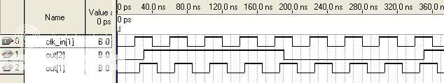
In my design I used the same output pins that were used in the working NIOS project. I just did a timing simulation and was able to see that my counter was working as expected. I've attached the schematic and the results below.
Thanks http://i560.photobucket.com/albums/ss46/creeg2/schematic.jpg http://i560.photobucket.com/albums/ss46/creeg2/simresult.jpg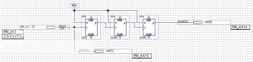
- Mark as New
- Bookmark
- Subscribe
- Mute
- Subscribe to RSS Feed
- Permalink
- Report Inappropriate Content
--- Quote Start --- In my design I used the same output pins that were used in the working NIOS project. I just did a timing simulation and was able to see that my counter was working as expected. I've attached the schematic and the results below. Thanks http://i560.photobucket.com/albums/ss46/creeg2/schematic.jpg http://i560.photobucket.com/albums/ss46/creeg2/simresult.jpg --- Quote End --- Hi, on the schematic I don't see any reason, why it should not work. Can you post the whole project? What kind of Quartus version did you use ? If you have a version which includes signaltap, try to tap one of your internal signals in order to make sure that the design is loaded. Kind regards GPK
- Mark as New
- Bookmark
- Subscribe
- Mute
- Subscribe to RSS Feed
- Permalink
- Report Inappropriate Content
So it appears there is a problem loading the design onto the FPGA. When I tried to use signal tap on my design, Quartus responded saying "Error: Can't find the instance. Download a design with SRAM Object File containing this instance.".
I suppose this means the design is not being loaded. When I ran SignalTap on the NOIS design I was able to see all of the output signals without any issue. So I guess this means the question has now moved to what is wrong with loading the design to the FPGA. I'll try to look for some differences between the NIOS design and my design but I definitely could use some guidance. Thanks for the signal tap hint. p.s. quartus version is: 7.2- Mark as New
- Bookmark
- Subscribe
- Mute
- Subscribe to RSS Feed
- Permalink
- Report Inappropriate Content
--- Quote Start --- So it appears there is a problem loading the design onto the FPGA. When I tried to use signal tap on my design, Quartus responded saying "Error: Can't find the instance. Download a design with SRAM Object File containing this instance.". I suppose this means the design is not being loaded. When I ran SignalTap on the NOIS design I was able to see all of the output signals without any issue. So I guess this means the question has now moved to what is wrong with loading the design to the FPGA. I'll try to look for some differences between the NIOS design and my design but I definitely could use some guidance. Thanks for the signal tap hint. p.s. quartus version is: 7.2 --- Quote End --- Hi, can you post your small project, I will have a look to it. Kind regards GPK
- Mark as New
- Bookmark
- Subscribe
- Mute
- Subscribe to RSS Feed
- Permalink
- Report Inappropriate Content
Here is the project I've made myself which I can't seem to get loaded onto the FPGA.
https://netfiles.uiuc.edu/creeg2/shared/clockout.zip Here is the hardware info again too: FPGA: EP2C35F484C6N mounted on a FireflyII module: http://www.microtronix.com/products/?product_id=86 Thanks! -Chris- Mark as New
- Bookmark
- Subscribe
- Mute
- Subscribe to RSS Feed
- Permalink
- Report Inappropriate Content
I think I resolved this issue. Looking though the Knowledge database:
http://www.altera.com/support/kdb/solutions/rd03212006_5.html It doesn't really explain it though. Does anyone know why this is a solution?- Mark as New
- Bookmark
- Subscribe
- Mute
- Subscribe to RSS Feed
- Permalink
- Report Inappropriate Content
Looks like a hardware bug in the dev board but they don't admit it, must be some unused pins are physically connected somewhere...
- Subscribe to RSS Feed
- Mark Topic as New
- Mark Topic as Read
- Float this Topic for Current User
- Bookmark
- Subscribe
- Printer Friendly Page