- Mark as New
- Bookmark
- Subscribe
- Mute
- Subscribe to RSS Feed
- Permalink
- Report Inappropriate Content
Hi all,
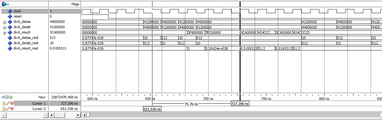
I'm considering using the floading point blocks available from Altera in a design I have. Throughput is a top priority as I'm doing complex image transformation for high speed application. I was trying out the altfp_div megafunction and found out that it outputs only correct answers every other clock cycle, possibly worse as I only tried it with two numbers. Is the altfp_div not fully pipelined? I saw this also with latency set to 14. I have added figures with this where div6rest_result is the correct values and div6_result_real is the value form the altfp_div. I also did the same for the altfp_inv floating point inverter. It seems to output correct values when receiving data every cycle. I also added a zip file with this test made in Quartus 9.1 Cheers Stefan p.s. Second question I have is are those megafunctions free to use with the web edition?Link Copied
- Mark as New
- Bookmark
- Subscribe
- Mute
- Subscribe to RSS Feed
- Permalink
- Report Inappropriate Content
It looks like your input data is changing on the rising edge of the clock.
This is not safe. Can you try again ensuring that the input data is changing of the falling edge of the clock?- Mark as New
- Bookmark
- Subscribe
- Mute
- Subscribe to RSS Feed
- Permalink
- Report Inappropriate Content
All data in the testbench waits for the rising edge of the clock, so input should be safe.
- Mark as New
- Bookmark
- Subscribe
- Mute
- Subscribe to RSS Feed
- Permalink
- Report Inappropriate Content
There's something I don't understand.
I run a simulation of your circuit using the attached testbench. If I read weel you're doing the operation 10/512=0.19... and 512/10 =51.2. I used your function : div6_result_real <= float32ToReal(div6_result); to display the results and it looks correct. You can run the simulation and let me know.- Mark as New
- Bookmark
- Subscribe
- Mute
- Subscribe to RSS Feed
- Permalink
- Report Inappropriate Content
- Mark as New
- Bookmark
- Subscribe
- Mute
- Subscribe to RSS Feed
- Permalink
- Report Inappropriate Content
P.S. I forgot to say that I changed the testbench and now the data is changing on the falling edge of the clock.
- Mark as New
- Bookmark
- Subscribe
- Mute
- Subscribe to RSS Feed
- Permalink
- Report Inappropriate Content
In a real system the input for a Flip Flop has to be stable for an interval of time before the active edge of the clock. This time is namd Setup Time (ts) and depends on the technology and the design of the Flip Flop.
In most simulations, it is safe to let the input data change on the falling edge of the clock, if the flip flop is triggered on the rising edge of the clock. In the real system, the input will be generated by another flip flop with combinational logic. The relation that has to be verified is the setup constraint that is: T > tq +Tc.max + ts Where: T = Clock period tq = flip flop delay ts = setup time Tc,max = the maximum combinational delay of the logic between the flip flops.- Mark as New
- Bookmark
- Subscribe
- Mute
- Subscribe to RSS Feed
- Permalink
- Report Inappropriate Content
Hi nplttr,
I'm fully aware of this. My experience is 3 years ASIC design (front-end and back-end design) and ~1 year FPGA design with Altera devices. In this example when I use the rising edge then the data has a full clock cycle to become stable before it is registered into the divider. How ever if I use falling edge the data only has half a cycle... I prefer to keep my design synced on rising edge unless I have a really good reason to switch over to falling edge. To place this buffer into the design will also cost my 64 registers + some additional logic. I wander if this is a bug in the behavioural code for the divider and if I have to do a gate level simulation for this... Cheers Stefan- Mark as New
- Bookmark
- Subscribe
- Mute
- Subscribe to RSS Feed
- Permalink
- Report Inappropriate Content
As I previously checked, setting the data at the rising edge gives correct results in a timing simulation, e.g. using Quartus V9 simulator. That's what you also can expect in a real device, because FPGA registers have a zero hold time requirement.
The ModelSim results are with functional simulation however, which is apparently causing the problems. At first sight, I wanted to agree with Tricky: --- Quote Start --- All data in the testbench waits for the rising edge of the clock, so input should be safe. --- Quote End --- But it this actually true? The VHDL specifation guarantees, that a process is "executed" completely, before the signals are updated. The execution order of multiple processes is however undefined. Also we don't know, how altfp_div is organized internally. Possibly combinational logic is placed before the first register level. If the code is not well considered, simulation artefacts may occur, effectively creating pathes of different length in terms of simulation delta cycles up to the first register. This won't matter in synthesized logic, when actual LE delays apply. If it's so, the suggestion to set the data on falling edge, or generally a few simulation time steps away from active clock edge, will help. P.S.: --- Quote Start --- I wander if this is a bug in the behavioural code for the divider --- Quote End --- Yes, I suppose so. It should be avoidable by better considering delta cycle delays.- Mark as New
- Bookmark
- Subscribe
- Mute
- Subscribe to RSS Feed
- Permalink
- Report Inappropriate Content
--- Quote Start --- Hi nplttr, I'm fully aware of this. My experience is 3 years ASIC design (front-end and back-end design) and ~1 year FPGA design with Altera devices. In this example when I use the rising edge then the data has a full clock cycle to become stable before it is registered into the divider. How ever if I use falling edge the data only has half a cycle... I prefer to keep my design synced on rising edge unless I have a really good reason to switch over to falling edge. To place this buffer into the design will also cost my 64 registers + some additional logic. I wander if this is a bug in the behavioural code for the divider and if I have to do a gate level simulation for this... Cheers Stefan --- Quote End --- You don't have to change the edge of the clock that produces the data. It will work. If you want to have an RTL simulation that is consistent with the real device, let the input data change silightly before the edge of the clock that registers it.
- Mark as New
- Bookmark
- Subscribe
- Mute
- Subscribe to RSS Feed
- Permalink
- Report Inappropriate Content
Hi FvM,
I agree with you and suppose this is due to delta delays in the simulator. I have used simulator resolution 1ps and 1ns with the same resaults. This will then make my design fail in RTL simulation, but work in gatelevel and on the real FPGA... This is fairly annoying and not making me very confident about this... makes me wander if there is something else not done properly. Doing a full simulation on the divider in not realistic as trying all possible inputs will take years in simulation time... How well are those blocks tested by Altera and can I trust them if I have no timing warnings when I verify my design with TimeQuest? Cheers Stefan- Mark as New
- Bookmark
- Subscribe
- Mute
- Subscribe to RSS Feed
- Permalink
- Report Inappropriate Content
--- Quote Start --- If you want to have an RTL simulation that is consistent with the real device, let the input data change silightly before the edge of the clock that registers it. --- Quote End --- How do you suggest doing this in synthesizableRTL code?
- Mark as New
- Bookmark
- Subscribe
- Mute
- Subscribe to RSS Feed
- Permalink
- Report Inappropriate Content
I would expect, that Altera is mainly focussing on synthesis performance. I also won't expect issues in the timing analysis.
The latest after Altera abandonned the internal simulator in favor of ModelSim, one should expect simulation proof IP code. Having the timing intentionally set in a test case is only the most obvious case. Normally, the data to altfp_mult would be supplied after rising clock edge from a register burried deep in the code. I guess some experience of the latter kind motivated your tests? So you should file a service request, I'm curious to hear the answer. In the meanwhile, you could try how many simulation time steps of additional delay in your test bench can make the artefact vanish.- Mark as New
- Bookmark
- Subscribe
- Mute
- Subscribe to RSS Feed
- Permalink
- Report Inappropriate Content
--- Quote Start --- How do you suggest doing this in synthesizableRTL code? --- Quote End --- I do not suggest to do this in synthesizable RTL Code. I suggest to do this in testbench. Testbenches are not for synthesys and it is your decision when to let the input data change.
- Mark as New
- Bookmark
- Subscribe
- Mute
- Subscribe to RSS Feed
- Permalink
- Report Inappropriate Content
--- Quote Start --- I would expect, that Altera is mainly focussing on synthesis performance. I also won't expect issues in the timing analysis. The latest after Altera abandonned the internal simulator in favor of ModelSim, one should expect simulation proof IP code. Having the timing intentionally set in a test case is only the most obvious case. Normally, the data to altfp_mult would be supplied after rising clock edge from a register burried deep in the code. I guess some experience of the latter kind motivated your tests? So you should file a service request, I'm curious to hear the answer. In the meanwhile, you could try how many simulation time steps of additional delay in your test bench can make the artefact vanish. --- Quote End --- I don't think this is an artifact. The edge of the clock and the data change simultaneously. How should the simulator decide which is the actual input of the flip flop in an RTL simulation? in a timing simulation the situation is different. there you can check for setup and hold times. I think this is one of the cases in which the result of the simulation depends on the simulator. In general, letting data and clock edge change at the same time, is asking for trouble.
- Mark as New
- Bookmark
- Subscribe
- Mute
- Subscribe to RSS Feed
- Permalink
- Report Inappropriate Content
--- Quote Start --- I don't think this is an artifact. The edge of the clock and the data change simultaneously. How should the simulator decide which is the actual input of the flip flop in an RTL simulation? in a timing simulation the situation is different. there you can check for setup and hold times. I think this is one of the cases in which the result of the simulation depends on the simulator. In general, letting data and clock edge change at the same time, is asking for trouble. --- Quote End --- Well this is actually wrong The synthesis and clock tree generation will take care of this. Gate level simulation is used to verify the clock tree is buffered correctly and that the design does not brake setup/hold times. Running in max/min corners will assure you don't brake the setup/hold times. If you would be hand-placing the block into the FPGA then you would use falling->rising edge or to protect your design for metastability between Analog World and FPGA or crossing clock domains...
- Mark as New
- Bookmark
- Subscribe
- Mute
- Subscribe to RSS Feed
- Permalink
- Report Inappropriate Content
This is a delta-delay issue like FvM mention. I added 1ps to the rising_edge and the divider works.
I'm installing version 10.1sp1 of the tools to see if this is the same there...- Mark as New
- Bookmark
- Subscribe
- Mute
- Subscribe to RSS Feed
- Permalink
- Report Inappropriate Content
--- Quote Start --- How should the simulator decide which is the actual input of the flip flop in an RTL simulation? --- Quote End --- VHDL has clear rules for it. Actually, most of the VHDL rules for "order of execution" are only relevant for simulation. In synthesis, logic delays clear most possible doubts, if timing closure can be achieved, everything is fine. Please notice, that the testbench code
wait until risind_edge(clk);
data <= xxx;
is simply identical to the behavioral code for a register in the data path. So if altfp_div fails with the testbench, it must be expected to fail in functional simulation with a simple register, too. Which means, you can't perform a functional simulation, as the original poster mentioned.
- Mark as New
- Bookmark
- Subscribe
- Mute
- Subscribe to RSS Feed
- Permalink
- Report Inappropriate Content
I tested this with altfp_div generated in 10.1sp1 and ModelSim 6.6d. It also fails there also. I will try to send service request to Atlera and see what they think.
Thanks all for the help Cheers Stefan- Mark as New
- Bookmark
- Subscribe
- Mute
- Subscribe to RSS Feed
- Permalink
- Report Inappropriate Content
- Subscribe to RSS Feed
- Mark Topic as New
- Mark Topic as Read
- Float this Topic for Current User
- Bookmark
- Subscribe
- Printer Friendly Page