- Mark as New
- Bookmark
- Subscribe
- Mute
- Subscribe to RSS Feed
- Permalink
- Report Inappropriate Content
I am using a 10M sram_clk to write data to the ssram on C3-starter-kit board.
The inside clk has a 180 degree phrase compared to sram_clk. I wrote data in single cycle and read in three cycles.But what i got from the read in register is not what i expected. I can not find error in my code.Can anybody help?This has been bothering for a week.Thank you. The attached file is the stp file. module memory (input wire iCLK_50, output reg [18:0] oSRAM_A, output reg oSRAM_ADSC_N, // controller address status output wire [ 3:0] oSRAM_BE_N, // byte write enable output wire oSRAM_CE1_N, // chip enable inout wire [31:0] SRAM_DQ, output reg oSRAM_OE_N, // output enable output reg oSRAM_WE_N , // write enable output wire LED1, output reg LED4 = 1, output reg [31:0] DATA_TMP, input wire KEY4, input wire rst ); reg SRAM_D_ena; reg [31:0] SRAM_D; reg [3:0] state; reg [3:0] key_state; reg [18:0] wp; reg [31:0] data; assign SRAM_DQ = SRAM_D_ena ? SRAM_D : 32'hZ; assign LED1 = (DATA_TMP == 32'h00000006) ? 0 : 1; assign oSRAM_BE_N = 4'd0; assign oSRAM_CE1_N= 0; always @(posedge iCLK_50 or negedge rst) //siginal tap trigger begin if(rst == 1'd0) LED4 <= 1'b1; else if(KEY4 == 0) LED4 <= 1'b0; else ; end always @(posedge iCLK_50 or negedge rst) begin if(rst == 1'd0) begin state <= 4'd11; wp <= 32'd0; DATA_TMP <= 32'hz; SRAM_D <= 32'h00000000; SRAM_D_ena <= 1'b0; oSRAM_ADSC_N <= 1; oSRAM_WE_N <= 1; oSRAM_OE_N <= 1; // close the SSRAM DQ drivers SRAM_D_ena <= 1; // be ready for writing end else if (LED4 == 1'b1) state <= 4'd11; else case (state) 11: begin oSRAM_ADSC_N <= 0; oSRAM_A <= wp; oSRAM_WE_N <= 0; wp <= wp+ 32'd1; SRAM_D <= SRAM_D+1; // WRITE! state <= 1; if(wp<6) begin state <= 11; end else begin state <=1; end end 1: begin // wait a cycle just in case state <= 2; SRAM_D_ena <= 0; // Turn off the drivers oSRAM_WE_N <= 1; end 2: begin // issue read oSRAM_ADSC_N <= 1; //single read state <= 3; oSRAM_OE_N <= 0; // Open the SSRAM drivers oSRAM_A <= 32'd2; //choose an address : 1 end 3: begin state <= 4; end// READ latency 4: begin state <= 5; end// READ latency 5: begin // receive data DATA_TMP <= SRAM_DQ; // READ! state <= 6; end 6: begin state <=6; end default: state<=6; endcase end endmodule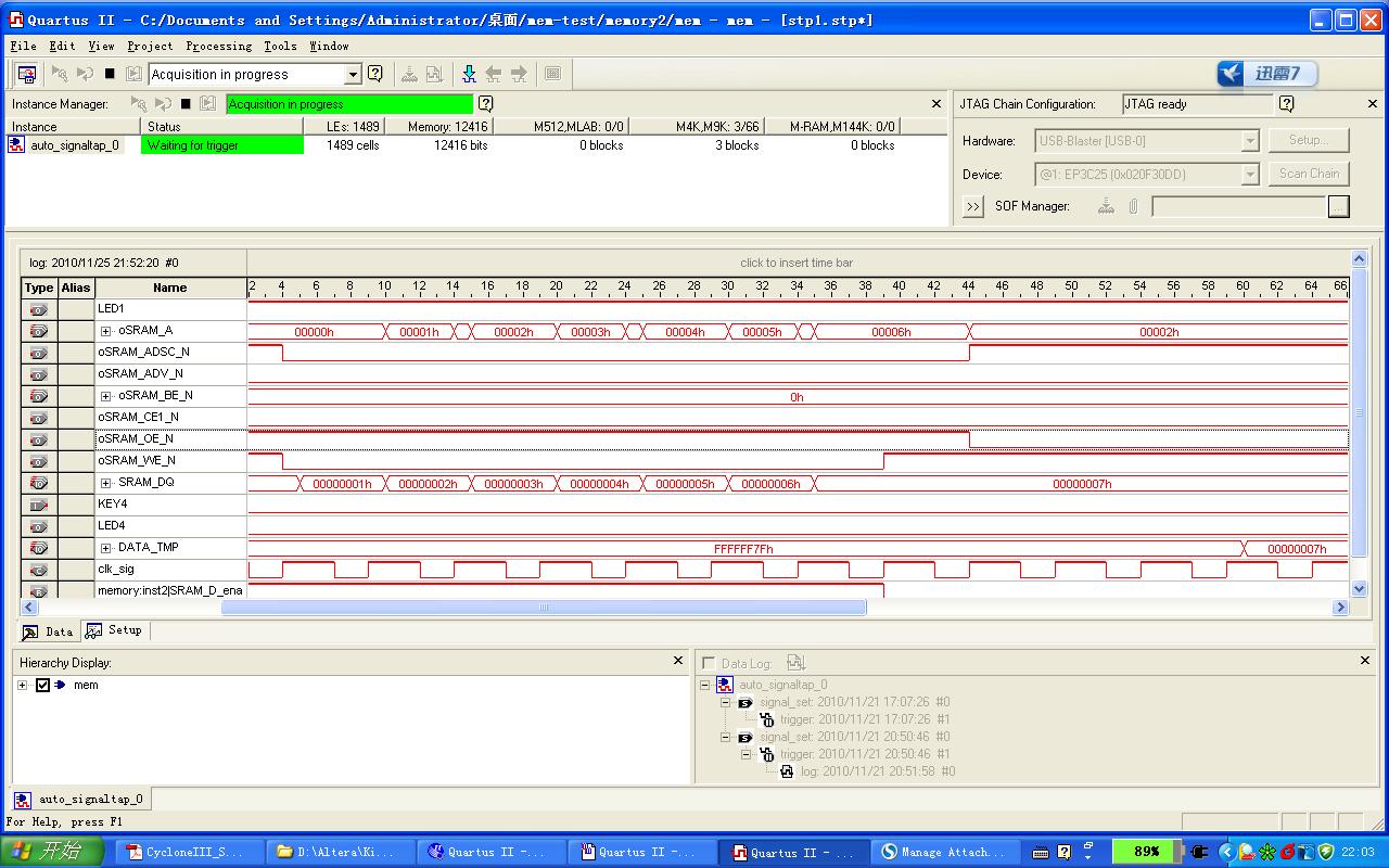
Link Copied
2 Replies
- Mark as New
- Bookmark
- Subscribe
- Mute
- Subscribe to RSS Feed
- Permalink
- Report Inappropriate Content
I haven't checked the datasheet, but shouldn't you keep ADSC low for one more cycle so that the SRAM gets your new read address?
- Mark as New
- Bookmark
- Subscribe
- Mute
- Subscribe to RSS Feed
- Permalink
- Report Inappropriate Content
--- Quote Start --- I haven't checked the datasheet, but shouldn't you keep ADSC low for one more cycle so that the SRAM gets your new read address? --- Quote End --- Thank you,Daixiwen Yes,i got right data when i keep ADSC low before read. The ADSP_n is pull up to high.I thought i could use single read model,but not.I got right at pipelined read model.
Reply
Topic Options
- Subscribe to RSS Feed
- Mark Topic as New
- Mark Topic as Read
- Float this Topic for Current User
- Bookmark
- Subscribe
- Printer Friendly Page