- Mark as New
- Bookmark
- Subscribe
- Mute
- Subscribe to RSS Feed
- Permalink
- Report Inappropriate Content
Link Copied
- Mark as New
- Bookmark
- Subscribe
- Mute
- Subscribe to RSS Feed
- Permalink
- Report Inappropriate Content
Hi,
Testbench module is defined without ports & used for functionality check/simulation of the design(using simulation tools) which is defined with input & output ports so compile the design, perform pin assignments & generate programming files for the design using full compilation & eventually load into the kit.
please refer the below link for reference.
https://www.youtube.com/watch?v=j5RGAW72o6A
Regards,
Vicky
- Mark as New
- Bookmark
- Subscribe
- Mute
- Subscribe to RSS Feed
- Permalink
- Report Inappropriate Content
Thank you
I already did all this things but I don't have any result on my scoope
- Mark as New
- Bookmark
- Subscribe
- Mute
- Subscribe to RSS Feed
- Permalink
- Report Inappropriate Content
Hi,
Could you please elaborate more about your observation with below points?
- pin assignment for clock, IOs etc
- successful compilation/programming file generation
- Device detection & successful program in Intel programmer
- observation of status LEDs.
Regards,
Vicky
- Mark as New
- Bookmark
- Subscribe
- Mute
- Subscribe to RSS Feed
- Permalink
- Report Inappropriate Content
Hi,
Have you resolved the issue?
May I know any update or Should I consider that case to be closed?
Regards,
Vicky
- Mark as New
- Bookmark
- Subscribe
- Mute
- Subscribe to RSS Feed
- Permalink
- Report Inappropriate Content
Hi,
the issue in not resolved I don't know the problem where I tried everything...all the point that you listed is done.
thank you
- Mark as New
- Bookmark
- Subscribe
- Mute
- Subscribe to RSS Feed
- Permalink
- Report Inappropriate Content
"Hi,
Could you please elaborate more about your observation with below points?
- pin assignment for clock, IOs etc
- successful compilation/programming file generation
- Device detection & successful program in Intel programmer
- observation of status LEDs.
Regards,
Vicky" ------------- it`s difficult to support without your inputs & observation so if possible provide at least all screenshots.
Regards,
Vicky
- Mark as New
- Bookmark
- Subscribe
- Mute
- Subscribe to RSS Feed
- Permalink
- Report Inappropriate Content
Thank you!
here it's my program :
LIBRARY ieee;
USE ieee.std_logic_1164.all;
USE ieee.std_logic_unsigned.all;
ENTITY pwm1 IS
GENERIC(
sys_clk : INTEGER := 100_000_000; --system clock frequency in Hz
pwm_freq : INTEGER := 600_000; --PWM switching frequency in Hz
bits_resolution : INTEGER := 8; --bits of resolution setting the duty cycle
phases : INTEGER := 4); --number of output pwms and phases
PORT(
clk : IN STD_LOGIC; --system clock
reset_n : IN STD_LOGIC; --asynchronous reset
ena : IN STD_LOGIC; --latches in new duty cycle
duty : IN STD_LOGIC_VECTOR(bits_resolution-1 DOWNTO 0); --duty cycle
pwm_out : OUT STD_LOGIC_VECTOR(phases-1 DOWNTO 0)); --pwm outputs
--pwm_n_out : OUT STD_LOGIC_VECTOR(phases-1 DOWNTO 0)); --pwm inverse outputs
END pwm1;
ARCHITECTURE logic OF pwm1 IS
CONSTANT period : INTEGER := sys_clk/pwm_freq; --number of clocks in one pwm period
TYPE counters IS ARRAY (0 TO phases-1) OF INTEGER RANGE 0 TO period - 1; --data type for array of period counters
SIGNAL count : counters := (OTHERS => 0); --array of period counters
SIGNAL half_duty_new : INTEGER RANGE 0 TO period/2 := 0; --number of clocks in 1/2 duty cycle
TYPE half_duties IS ARRAY (0 TO phases-1) OF INTEGER RANGE 0 TO period/2; --data type for array of half duty values
SIGNAL half_duty : half_duties := (OTHERS => 0); --array of half duty values (for each phase)
BEGIN
PROCESS(clk, reset_n)
BEGIN
IF(reset_n = '0') THEN --asynchronous reset
count <= (OTHERS => 0); --clear counter
pwm_out <= (OTHERS => '0'); --clear pwm outputs
-- pwm_n_out <= (OTHERS => '0'); --clear pwm inverse outputs
ELSIF(clk'EVENT AND clk = '1') THEN --rising system clock edge
IF(ena = '1') THEN --latch in new duty cycle
half_duty_new <= conv_integer(duty)*period/(2**bits_resolution)/2; --determine clocks in 1/2 duty cycle
END IF;
FOR i IN 0 to phases-1 LOOP --create a counter for each phase
IF(count(0) = period - 1 - i*period/phases) THEN --end of period reached
count(i) <= 0; --reset counter
half_duty(i) <= half_duty_new; --set most recent duty cycle value
ELSE --end of period not reached
count(i) <= count(i) + 1; --increment counter
END IF;
END LOOP;
FOR i IN 0 to phases-1 LOOP --control outputs for each phase
IF(count(i) = half_duty(i)) THEN --phase's falling edge reached
pwm_out(i) <= '0'; --deassert the pwm output
--pwm_n_out(i) <= '0' after 100 ns; --assert the pwm inverse output
ELSIF(count(i) = period-half_duty(i)) THEN --phase's rising edge reached
pwm_out(i) <= '1';
--pwm_n_out(i) <= '1' after 100 ns; --assert the pwm output
--deassert the pwm inverse output
END IF;
END LOOP;
END IF;
END PROCESS;
END logic;
- Mark as New
- Bookmark
- Subscribe
- Mute
- Subscribe to RSS Feed
- Permalink
- Report Inappropriate Content
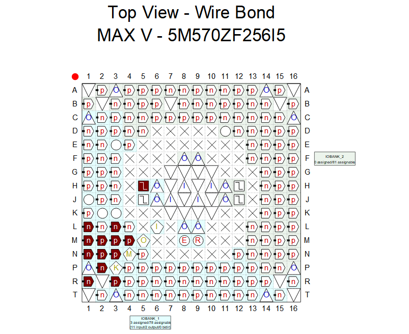
here it's my pin assignment
- Mark as New
- Bookmark
- Subscribe
- Mute
- Subscribe to RSS Feed
- Permalink
- Report Inappropriate Content
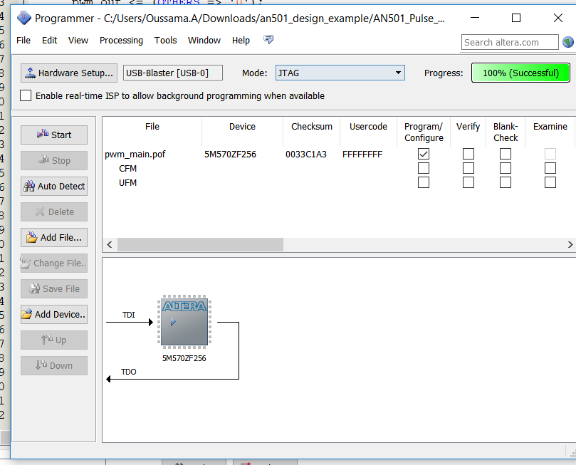
I'm generating the compilation/programming file very well and the device is programmed via usb blaster
- Subscribe to RSS Feed
- Mark Topic as New
- Mark Topic as Read
- Float this Topic for Current User
- Bookmark
- Subscribe
- Printer Friendly Page

