- Mark as New
- Bookmark
- Subscribe
- Mute
- Subscribe to RSS Feed
- Permalink
- Report Inappropriate Content
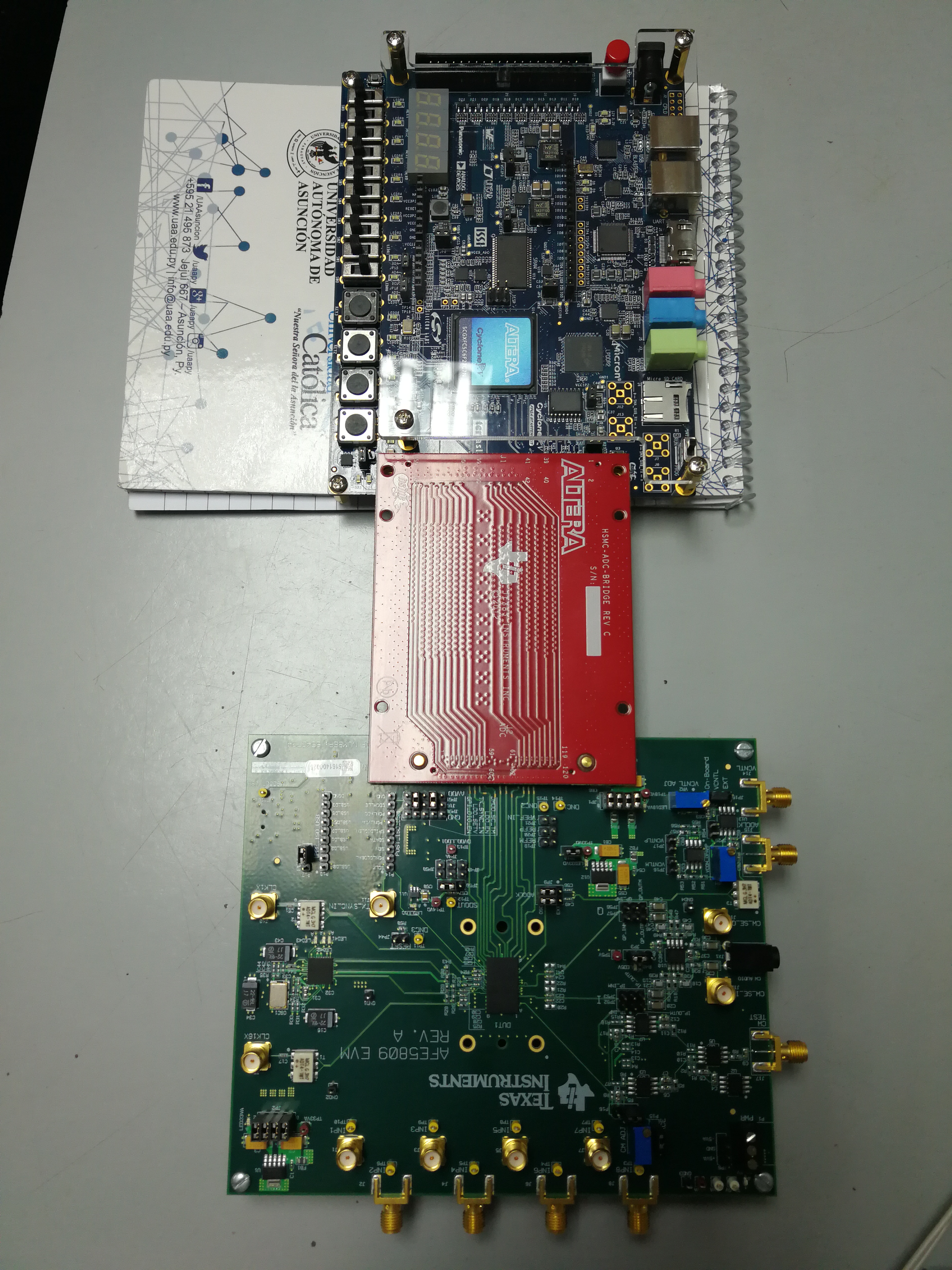
Few weeks ago I aquire the cyclone V GX starter kit, we are working in a project using the AFE5809evm to receive data from a array of ultrasound sensors, the AFE do all the signal digitalize and give the values via LVDS signal by and HSMC port. I need to interface this LVDS to FPGA(cyclone V GX)
- If anybody can help me to understand better the situation.
- It will be greatful if you guys can provide me as much information as possible, how to receive this LVDS signal through HSMC in order to have the LVDS to single ended.
Finally, I saw in another post that I can directly interface the LVDS channels to this FPGA but I and no quite familiarize with this FPGA and I do not know how to do it.
- Do I need and specific and extensive code to do that?
Regards
Mateo Recalde
Link Copied
- Mark as New
- Bookmark
- Subscribe
- Mute
- Subscribe to RSS Feed
- Permalink
- Report Inappropriate Content
- Mark as New
- Bookmark
- Subscribe
- Mute
- Subscribe to RSS Feed
- Permalink
- Report Inappropriate Content
Thank you very much for providing specific tips on my problem, now I'm looking specifically for more information based on what you gave me, for example this video (https://www.youtube.com/watch?v=02lgfcxSjQA), if it has no relation to what you told me please let me know.
I hope to continue in permanent contact with you, since we are developing a project with the cyclone V GX starter kit and it is the first time that I am programming in it.
- Mark as New
- Bookmark
- Subscribe
- Mute
- Subscribe to RSS Feed
- Permalink
- Report Inappropriate Content
- Mark as New
- Bookmark
- Subscribe
- Mute
- Subscribe to RSS Feed
- Permalink
- Report Inappropriate Content
Thank you so much SOoYL for answer me,
Reading an old post here I realized that I obviously must assign the correct pin to each entry coming from the AFE5809evm to the FPGA through the HSMC-ADC-BRIDGE, I have them all assigned in paper, and using DIFFIO_RX_ I assign them one by one in the Quartus (Web edition 15.0), is that right ?.
On the other hand in the same post it mentions that the FPGA will convert the differential signal to single-ended internally at the IOBUFF level. What I do not understand is how to use the command mentioned above.
In the Quartus I create a new project, I am very sorry but it is my second project in this, I go to the assignment's window -> pins planner -> differential Pins -> DIFF Input with serdes, there I have all the pins available to be assigned, What I found is that the pin corresponding to FCLKM(LVDS frame clock x1 negative output) and FCLKP(LVDS frame clock x1 positive output) of the AFE5809evm will be connected to the HSMC_RXp16 / n16 pins respectively, would this be a problem in the future for the correct reading of the data?
Those are all the signals I need por process :
- D1M to D8M ADC CH1 to CH8 LVDS negative output
- D1P to D8P ADC CH1 to CH8 LVDS positive output
- DCLKM LVDS bit clock (7x) negative output
- DCLKP LVDS bit clock (7x) positive output

In the figure we observe the corresponding pins to be received called DKp/m where K is the number of signals (8) and p/n positive and negative respectively.
Again I ask for mercy, since I find it very difficult to program in this language using the QUARTUS.
Regards,
Mateo
- Mark as New
- Bookmark
- Subscribe
- Mute
- Subscribe to RSS Feed
- Permalink
- Report Inappropriate Content
Hi Mateo,
Please find my response below:
1.Reading an old post here I realized that I obviously must assign the correct pin to each entry coming from the AFE5809evm to the FPGA through the HSMC-ADC-BRIDGE, I have them all assigned in paper, and using DIFFIO_RX_ I assign them one by one in the Quartus (Web edition 15.0), is that right ?.
Yes, correct.
2.On the other hand in the same post it mentions that the FPGA will convert the differential signal to single-ended internally at the IOBUFF level. What I do not understand is how to use the command mentioned above.
In the Quartus I create a new project, I am very sorry but it is my second project in this, I go to the assignment's window -> pins planner -> differential Pins -> DIFF Input with serdes, there I have all the pins available to be assigned, What I found is that the pin corresponding to FCLKM(LVDS frame clock x1 negative output) and FCLKP(LVDS frame clock x1 positive output) of the AFE5809evm will be connected to theHSMC_RXp16 / n16 pins respectively, would this be a problem in the future for the correct reading of the data?
You will need to configure the pin in pin planner to differential I/O Standard (LVDS and etc) depending on the pin. In order to do the "differential signal to single-ended", it might need to use our LVDS serdes IP. Please refer to link below for more information about the IP.
https://www.intel.com/content/dam/www/programmable/us/en/pdfs/literature/ug/ug_altlvds.pdf
Hope it helps.
Regards,
YL
- Subscribe to RSS Feed
- Mark Topic as New
- Mark Topic as Read
- Float this Topic for Current User
- Bookmark
- Subscribe
- Printer Friendly Page