- Mark as New
- Bookmark
- Subscribe
- Mute
- Subscribe to RSS Feed
- Permalink
- Report Inappropriate Content
Hi, I am new with Quartus designs and have following questions to compiler reports. There are no errors but many warnings.
1) I designed a schematic with the block editor. Compilation for a MAX3000A, EPM3064ATC44, needs 58 macrocells and 33 pins.
But compilation for a MAX II, EPM240T100, only needs 37 logic elements and 29 pins.
I know that a LE of EPM240 is more complex than a macrocell of MAX3000A, but the difference is very large. Also I don't understand why for an EPM3064A there are 4 pins more needed than the schematic contains. There are only 29 inputs/outputs.
2) For the EPM3064A I get 4 warnings about combinational loops:
Warning (332125): Found combinational loop of 2 nodes
Warning (332126): Node "inst11|7~6|[2]"
Warning (332126): Node "inst11|7~6|dataout"
Warning (332125): Found combinational loop of 2 nodes
Warning (332126): Node "inst11|8~6|[2]"
Warning (332126): Node "inst11|8~6|dataout"
Warning (332125): Found combinational loop of 2 nodes
Warning (332126): Node "inst11|9~6|[2]"
Warning (332126): Node "inst11|9~6|dataout"
Warning (332125): Found combinational loop of 2 nodes
Warning (332126): Node "inst11|10~6|[2]"
Warning (332126): Node "inst11|10~6|dataout"
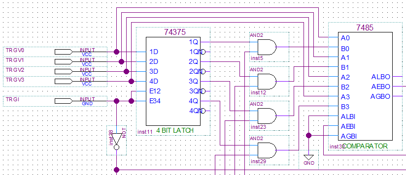
The part of the schematic with inst11 is attached.
How to interpret e.g. inst11|10~6|[2]?
I don't see a combinational loop with inst11. Where is it?
3) There are further messages I don't understand:
Warning (332060): Node: CLK was determined to be a clock but was found without an associated clock assignment.
Warning (332061): Virtual clock CLK is never referenced in any input or output delay assignment.
Really there is a clock input called CLK. The sdc file contains two lines:
set_time_format -unit ns -decimal_places 3
create_clock -name {CLK} -period 50.000 -waveform { 0.000 25.000 }
How and where shall I do an associated clock assignment?
What is about virtual clock? I didn't define it.
Link Copied
- Mark as New
- Bookmark
- Subscribe
- Mute
- Subscribe to RSS Feed
- Permalink
- Report Inappropriate Content
1) Different I/O requirements don't make sense unless you removed I/O signals from the design, unless other pins like power or JTAG are being counted. Without seeing the design or the report, it's not really possible to determine what's going on here.
2) You're using latches instead of registers which by their very nature are combinational loops.
3) Your SDC is wrong. You have no target for your clock input. It should be something like this (depending on the name of your clock input pin):
create_clock -name {CLK} -period 50.000 -waveform { 0.000 25.000 } [get_ports clk]
Without the target, you've created a virtual clock, a clock created outside the FPGA that never actually enters the device, used for I/O timing analysis.
- Mark as New
- Bookmark
- Subscribe
- Mute
- Subscribe to RSS Feed
- Permalink
- Report Inappropriate Content
With question 1 I don't have a problem. Meantime I found that with EPM240T100 the compiler did not count the JTAG pins.
So questions 1 and 2 are solved.
For question 3 you say
Without the target, you've created a virtual clock, a clock created outside the FPGA that never actually enters the device, used for I/O timing analysis.
I don't know what the 'target' should be in my schematic. The pin planner connects the clock input named CLK to pin 37 of the chip named GCLK1. So CLK is entering the device. This part of my schematic is shown in the attachment.
I tried to extend the corresponding line within the sdc file according to your example:
create_clock -name {CLK} -period 50.000 -waveform { 0.000 25.000 } [get_ports GCLK1]
but the new compiler report contains the message
Warning (332174): Ignored filter at myTest.out.sdc(41): GCLK1 could not be matched with a port
I guess that the compiler will generate VHDL code from the schematic and in this code CLK is connected to a name which is the 'target'. But I don't know this name because I have no VHDL code for it. I only have the schematic.
Can you please give me tips how to find the needed 'target'?
- Mark as New
- Bookmark
- Subscribe
- Mute
- Subscribe to RSS Feed
- Permalink
- Report Inappropriate Content
I don't see a clock input in the part of your schematic you attached unless you're talking about "TRGI". The target should be whatever you've named it in the design. If it's TRGI, use that.
VHDL code has nothing to do with this. The tool interprets the schematic directly.
- Mark as New
- Bookmark
- Subscribe
- Mute
- Subscribe to RSS Feed
- Permalink
- Report Inappropriate Content
In my former post I had attached a further image showing the clock input of my schematic but it was not transfered.
I try it again hoping that it will be transfered now.
- Mark as New
- Bookmark
- Subscribe
- Mute
- Subscribe to RSS Feed
- Permalink
- Report Inappropriate Content
if it's the top level schematic, the clock pin name is set to "CLK" by applying the name to the pin symbol. It has to be referenced in get_ports.
- Mark as New
- Bookmark
- Subscribe
- Mute
- Subscribe to RSS Feed
- Permalink
- Report Inappropriate Content
So, yes, it should be [get_ports CLK] in your create_clock command.
- Mark as New
- Bookmark
- Subscribe
- Mute
- Subscribe to RSS Feed
- Permalink
- Report Inappropriate Content
Hi,
Do the above comments help?
Regards,
Nurina
- Mark as New
- Bookmark
- Subscribe
- Mute
- Subscribe to RSS Feed
- Permalink
- Report Inappropriate Content
Hi,
We have not received a reply from you. As such, I now transition this thread to community support. If you have a new question, Feel free to open a new thread or login to ‘ https://supporttickets.intel.com ’, view details of the desire request, and post a feed/response within the next 15 days to allow me to continue to support you. After 15 days, this thread will be transitioned to community support. The community users will be able to help you on your follow-up questions.
If any answer from the community or Intel Support are helpful, feel free to rank your support experience by rating 4/5 survey. Please let me know of any inconvenience so that I may improve your future service experience.
Have a great day!
Best regards,
Nurina W.
p/s: If any answer from the community or Intel Support are helpful, please feel free to give best answer or rate 4/5 survey.
- Subscribe to RSS Feed
- Mark Topic as New
- Mark Topic as Read
- Float this Topic for Current User
- Bookmark
- Subscribe
- Printer Friendly Page