- Mark as New
- Bookmark
- Subscribe
- Mute
- Subscribe to RSS Feed
- Permalink
- Report Inappropriate Content
Hi,
Could someone tell me how to use/connect the 4 clocks of the max V device KIT? As in the datasheet, there are 4 clocks which are located at pin H5, J5, H12, J12. The pin H5 is used for the external 10MHz clock. Now I have other 3 external clocks and I want to connect these clocks as inputs to the Max V KIT, however I cannot find where to connect theem to the board ? In the datasheet, it says that both pin H12 and pin J12 are located at J9.1 of the board. But I do not understand how can i use a single physical connector for 2 clock signals ? Here is the board http://www.alteraforum.com/forum/attachment.php?attachmentid=12392&stc=1 Thanks Bien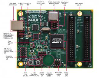
Link Copied
1 Reply
- Mark as New
- Bookmark
- Subscribe
- Mute
- Subscribe to RSS Feed
- Permalink
- Report Inappropriate Content
Refer to the schematic that comes with the documentation. J5 isn't broken out. H12 & J12 are presented on J9 pin 1. However, driving this will mean you end up driving both H12 & J12 (and some other I/O pins), unless you remove some resistors.
Cheers, Alex
Reply
Topic Options
- Subscribe to RSS Feed
- Mark Topic as New
- Mark Topic as Read
- Float this Topic for Current User
- Bookmark
- Subscribe
- Printer Friendly Page