- Mark as New
- Bookmark
- Subscribe
- Mute
- Subscribe to RSS Feed
- Permalink
- Report Inappropriate Content
I have implemented a design using the Dual Configuration Core in a Max10 device. I can trigger a remote system update with the core successfully, but seem to be getting erroneous status when reading back from the core after a successful reconfiguration of the device.
Specifically, I program the flash (CFM1) and then trigger an RSU by writing 0x1 to offset 0x0 of the dual config core. I then wait the max time for the device to be programmed, and then read out a user defined version register that is part of the RTL design, and confirm that the device reconfigured successfully.
At that point, I write 0xF to dual config core offset 0x2, which should cause status registers at offsets 0x5 and 0x6 to update. The lower 4 bits of these status registers show reconfiguration sources should there be an interruption of device configuration (for CRC or assertion of nconfig etc). I seem to be getting non-zero status on these status bits, somewhat random values, immediately after an RSU. If however I power cycle the board and allow the max 10 (10M08) to cold boot the new flash image I get the expected 0x0 for these values.
So it seems I have some issue with status reporting on warm boots of 10M08 right after an RSU.
Link Copied
- Mark as New
- Bookmark
- Subscribe
- Mute
- Subscribe to RSS Feed
- Permalink
- Report Inappropriate Content
Hi,
Thank you for contacting intel community.
Per my understanding, you are using dual configuration IP with RSU.
What do you mean by erroneous status? Is there any error shown?
Have you refer to RSU userguide and also MAX10 userguide?
Regards,
Aiman
- Mark as New
- Bookmark
- Subscribe
- Mute
- Subscribe to RSS Feed
- Permalink
- Report Inappropriate Content
So I'm looking at the Dual Config Core registers at offset 5 and 6 which are defined as follow from the data sheet:
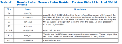
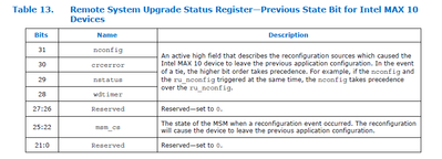
Specifically, I'm looking the Bit 3:0 in each register which defines what caused a reconfiguration of the device. If I understand correctly this would tell me in the event of some failure what caused it. The definition of these bits I'm taking from another part of the data sheet:
This is where the datasheet is confusing. As it seems the above table 13 is showing a status register from some internal logic in the device. Here I presumed that bits [31:28] which describe reconfiguration sources, are the same reconfiguration sources as in the Dual Config Core, just mapped into offsets 0x5 and 0x6 (bits [3:0] of the core avalon bus status registers.
I had presumed that these should all be 0 in the event of a successful RSU, which they indeed are when I cold boot the device. But on a warm boot, right after configuration, I seem to sometimes get a non-zero value on one or more of the 4 config sources (nconfig,crc error, nstatus, wdtimer), this is what I mean by erroneous status. But even here the device loaded successfully, so it looks like only a status reporting problem on a warm boot.
- Mark as New
- Bookmark
- Subscribe
- Mute
- Subscribe to RSS Feed
- Permalink
- Report Inappropriate Content
Have you had a chance to review my latest post above?
- Mark as New
- Bookmark
- Subscribe
- Mute
- Subscribe to RSS Feed
- Permalink
- Report Inappropriate Content
Hi,
Thanks for your patience. Got confirmation from internal team that Table 36 is incorrect. You are requested to refer to Table 13 for correct bit mapping.
The user guide will be fixed in future.
Regards
- Mark as New
- Bookmark
- Subscribe
- Mute
- Subscribe to RSS Feed
- Permalink
- Report Inappropriate Content
Hi,
Additional information here to be noted. Please refer Table 11 for offset 1 and Table 12 for offset 4.
Regards
- Mark as New
- Bookmark
- Subscribe
- Mute
- Subscribe to RSS Feed
- Permalink
- Report Inappropriate Content
I have a similar query and observations that the documentation for the Remote System Upgrade registers makes no sense.
Even the answer above that Tables 11, 12, and 13 somehow should make sense of these registers seems to be incorrect.
For example Table 11:
From observation it would seem that this is wrong since the only bits in register 1 that seem to be active are [1:0] and these seem to map into ru_boot_sel (bit 0) and ru_boot_sel_overwrite (bit 1). Moreover, that register is clearly not "Read Only" as but in fact RW. This seems to be an arbitrary mapping unrelated to this table.
For Table 12 (supposedly for offset 4):
I seem to only read back values of 0x00004FFF or 0x00008FFF. My design does not have the watch-dog enabled so I would expect that ru_wd_en is always zero. I would also expect that wd_timeout_value would be maximum and not changing. Now clearly the Avalon-MM register is only 32-bits wide so what we are supposed to interpret from a 34-bit wide table is beyond me. Based on the evident bit patterns I would have to guess that the actual register has some other mapping. The bits [31:16] seem to always be zero and the bits [15:0] do not seem to make sense since the only bits that should really change in my design might be the msm_cs bits and those are not seemingly in the right place.
For Table 13 (offsets 5 & 6):
I get a variety of values depending on the validity of CFM1/CFM0 and how the device was triggered to configure but these values are always non-zero bits in the LSB (e.g. [7:0]) like 0x00000028 or 0x00000058 or 0x00000044 etc. How those map into Table 13 is a mystery to me. I have yet to reverse engineer what the mapping might be.
So frankly I don't know how you could possibly think that
> the query has been answered
since as best I can tell, this is equally confusing and wrong. Is there some special bit ordering that is not evident? Does the document specify bits in some strange way such that perhaps the Most Significant Bit is 0 and the Least Significant Bit is 31 (or 33 or ???)
There is no driver header file to make sense of this.
There is no sample that demonstrates the interpretation of these bits.
The documentation is a complete falsehood.
How can anyone be expected to make any sense of this?
OP: Did you actually find an answer in this that allowed you to interpret the values in the status registers and figure out the state of the RU logic?
- Mark as New
- Bookmark
- Subscribe
- Mute
- Subscribe to RSS Feed
- Permalink
- Report Inappropriate Content
Hi,
As the query has been answered, I am closing this case. However, it will still be open form Community member to respond.
Regards
- Mark as New
- Bookmark
- Subscribe
- Mute
- Subscribe to RSS Feed
- Permalink
- Report Inappropriate Content
>The user guide will be fixed in future.
When?
Can Altera at least publish an accurate and complete bit layout of the registers in tabular form?
- Subscribe to RSS Feed
- Mark Topic as New
- Mark Topic as Read
- Float this Topic for Current User
- Bookmark
- Subscribe
- Printer Friendly Page


