- Mark as New
- Bookmark
- Subscribe
- Mute
- Subscribe to RSS Feed
- Permalink
- Report Inappropriate Content
My project has this warning
Warning: PLL "PLL:inst_PLL|altpll:altpll_component|PLL_altpll:auto_generated|pll1" input clock inclk[0] is not fully compensated and may have reduced jitter performance because it is fed by a non-dedicated input
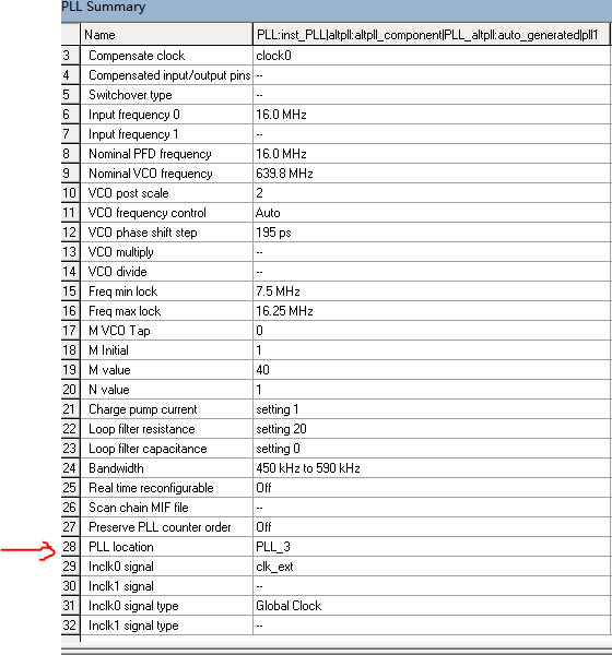
However, in my design the inst_PLL inclk[0] is feed by clk_ext whose location is at Pin_B9 which is a dedicated clock pin. Why the warning appears even though the PLl is already feeded by the dedicated clock pin?
- Tags:
- constraints
- pll
Link Copied
- Mark as New
- Bookmark
- Subscribe
- Mute
- Subscribe to RSS Feed
- Permalink
- Report Inappropriate Content
Hi,
Yes, you have used dedicated clock input pin. As per the recommended pin assignments in the Quartus II software for the PLL input is
- inclk[1,0] – dedicated clock input pin (CLK[15..0]) & you have used clk9.
Which PLL have been used? (PLL1,PLL2,PLL3 or PLL4?)
Assuming PLL1, try by selecting clock from CLK[3..0] or CLK[15..12] {PINS=E2,E1,M2,M1,R8,T8,R9,T9}
Check if you are getting same Warning.
Other recommendation.
The PLL input clock must be either dedicated input clock pins or another PLL output. The PLL input clock cannot be driven from internal logic. The PLL output clock should be connected to its dedicated clock output pin for optimum routing (only applies to c0), user I/O, or global clock (GCLK).
If you want compensation of the specified input clock or better jitter performance,connect the input clock only to an input pin, or assign the input pin only to a dedicated input clock location for the PLL.
If you do not want compensation of the specified input clock, then set the PLL to No Compensation mode.
Regards
Anand
- Mark as New
- Bookmark
- Subscribe
- Mute
- Subscribe to RSS Feed
- Permalink
- Report Inappropriate Content
“Which PLL have been used? (PLL1,PLL2,PLL3 or PLL4?) Assuming PLL1, try by selecting clock from CLK[3..0] or CLK[15..12] {PINS=E2,E1,M2,M1,R8,T8,R9,T9} Check if you are getting same Warning.”
-- I use CLK9 and the Quartus assign the PLL3 for it automatically. I have tried to assign the input clock pin location to other CLK, the warning is still there.
"The PLL input clock must be either dedicated input clock pins or another PLL output. The PLL input clock cannot be driven from internal logic. The PLL output clock should be connected to its dedicated clock output pin for optimum routing (only applies to c0), user I/O, or global clock (GCLK)."
-- The PLL input clock in this design is directly from the dedicated clock pin.
"If you want compensation of the specified input clock or better jitter performance,connect the input clock only to an input pin, or assign the input pin only to a dedicated input clock location for the PLL.
If you do not want compensation of the specified input clock, then set the PLL to No Compensation mode."
-- Yes, there is no combinational logic between the dedicated input clock pin and the PLL input. The PLL is set to Normal Mode because the PLL output is the system clock.
- Mark as New
- Bookmark
- Subscribe
- Mute
- Subscribe to RSS Feed
- Permalink
- Report Inappropriate Content
Is the clock pin feeding only the PLL or does it feed any other block in the design apart from the PLL.? sometimes this warning can occur if the input clock feeds another block apart from the PLL inclock.
- Subscribe to RSS Feed
- Mark Topic as New
- Mark Topic as Read
- Float this Topic for Current User
- Bookmark
- Subscribe
- Printer Friendly Page

