- Mark as New
- Bookmark
- Subscribe
- Mute
- Subscribe to RSS Feed
- Permalink
- Report Inappropriate Content
Hi,
UG-20007
2021.03.19
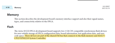
In the following section ( picture below), it says "These devices are part of the shared FM bus that connects to the flash memory and MAX V
CPLD EPM2210 System Controller."
Question : I believe EPM2210 is a MAX II CPLD. Why does the user guide says MAX V CPLD EPM2210?. Is this a typo in the user guide?. Can you please explain?
Link Copied
- Mark as New
- Bookmark
- Subscribe
- Mute
- Subscribe to RSS Feed
- Permalink
- Report Inappropriate Content
There's a MAX II for the onboard USB blaster and a MAX V (5M2210). See the schematic:
- Mark as New
- Bookmark
- Subscribe
- Mute
- Subscribe to RSS Feed
- Permalink
- Report Inappropriate Content
Hi sstrell,
Thanks for the response. I have further three more questions.
Q1) So the Max II CPLD is the system controller is it?
Q2) And also what is the usage of EPCQ1024L in page 14 of the schematic?.
Q3) I understand Max II & Max V are used for configuring the on board USB blaster, and control configuration of FPGA from flash respectively. Is my understanding correct?
Thank you.
- Mark as New
- Bookmark
- Subscribe
- Mute
- Subscribe to RSS Feed
- Permalink
- Report Inappropriate Content
2) I’m not at my computer now but that’s a configuration device with flash memory to store programming data.
3) yes.
- Mark as New
- Bookmark
- Subscribe
- Mute
- Subscribe to RSS Feed
- Permalink
- Report Inappropriate Content
Great!. The answers are clear. I am gonna shoot more basic questions to help me understand the specifics. Please bear with me.
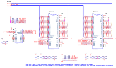
Now, moving further to how the 1-Gbit flash memory is connected, I see that there are two flash chips (u4), and (u5) in the schematic which shares an Address bus, and also two interesting notes in blue color at the bottom. (attaching picture below).
I would like to understand, why the connection in made in such a way with 2 flash memories?. Is there a specific reason?
And, what does the note in the blue signify?. I believe as per the schematic, I should focus on the 2nd note which mentions about dual flash device. Am I right?
- Mark as New
- Bookmark
- Subscribe
- Mute
- Subscribe to RSS Feed
- Permalink
- Report Inappropriate Content
You can access a single flash chip as x16 or use both to use a larger flash as x32.
- Mark as New
- Bookmark
- Subscribe
- Mute
- Subscribe to RSS Feed
- Permalink
- Report Inappropriate Content
Thanks, got that point.
I am intrigued on these statements. Can you possibly give a little bit more info on these?. I do not comprehend on the logic, intention behind it.
Thanks
- Subscribe to RSS Feed
- Mark Topic as New
- Mark Topic as Read
- Float this Topic for Current User
- Bookmark
- Subscribe
- Printer Friendly Page


