- Mark as New
- Bookmark
- Subscribe
- Mute
- Subscribe to RSS Feed
- Permalink
- Report Inappropriate Content
Hi
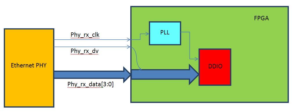
design: My design interfaces an RGMII Gigabit Ethernet running at 125 MHz with 4 bits of data and 1 bit for validity of data. Data & clock are edge-aligned at the PHY output ports: Data: GPHY_RXD[3:0] Data Validity: GPHY_RXCTL Clock: GPHY_RXCLK FPGA is receiver & PHY is transmitter. In order to constrain my design I have studied both source_synchronous_timing (http://www.alterawiki.com/uploads/e/ea/source_synchronous_timing.pdf) and an443 (https://www.google.com/url?sa=t&rct=j&q=&esrc=s&source=web&cd=1&cad=rja&uact=8&ved=0ahukewigmpbj8_vkahuk1xikhuosdf0qfggimaa&url=https%3a%2f%2fwww.altera.com%2fliterature%2fan%2fan433.pdf&usg=afqjcnf1ozxqltnqpgli66byyh3wngw7dw). I have instantiated a pll in the source synchronous compensation mode which is fed by GPHY_RXCLK. Its output clock is generated with a 90 degree phase shift, so that clock & data are center-aligned. The PLL output clock feeds the clock port of a ddio, generated by MegaWizard. GPHY_RXD and GPHY_RXCTL are also concatenated and feed the DDIO data port. I'm using Cyclone-III and Quartus-v11. http://www.alteraforum.com/forum/attachment.php?attachmentid=11830&stc=1 my constraints: I have mentioned all the constraints that are related to the Ethernet PHY. --- Quote Start --- # Input Clock create_clock -name {phy_rx_clock} -period 8.000 -waveform { 0.000 4.000 } [get_ports {GPHY_RXCLK}] #Virtual Clock for PHY create_clock -name phy_rx_clock_virtual -period 8.000 -waveform { 0.000 4.000 } # Generated Clocks derive_pll_clocks # Clock Uncertainty derive_clock_uncertainty # Input Delay set rgmii_input_delay_min -0.50 set rgmii_input_delay_max 0.50 set rgmii_mac_inputs [get_ports { GPHY_RXCTL GPHY_RXD [*] }] set_input_delay -clock phy_rx_clock_virtual -min $rgmii_input_delay_min $rgmii_mac_inputs set_input_delay -clock phy_rx_clock_virtual -max $rgmii_input_delay_max $rgmii_mac_inputs set_input_delay -clock phy_rx_clock_virtual -clock_fall -min $rgmii_input_delay_min $rgmii_mac_inputs -add_delay set_input_delay -clock phy_rx_clock_virtual -clock_fall -max $rgmii_input_delay_max $rgmii_mac_inputs -add_delay # Clock Groups set_clock_groups -asynchronous -group {clk_100_MHz} \ -group {u_Pll|altpll_component|auto_generated|pll1|clk[0]} \ -group {u_Pll|altpll_component|auto_generated|pll1|clk[1]} \ -group {u_Pll|altpll_component|auto_generated|pll1|clk[2]} \ -group {u_Pll|altpll_component|auto_generated|pll1|clk[3]} \ -group {u_pll_10_to_125|altpll_component|auto_generated|pll1|clk[0]} \ -group {u_pll_phy_rx_clk|altpll_component|auto_generated|pll1|clk[0]} \ -group {u_S1LL|altpll_component|auto_generated|pll1|clk[0]} \ -group {u_S1PLL|altpll_component|auto_generated|pll1|clk[1]} # False Paths set_false_path -fall_from phy_rx_clock_virtual -fall_to u_pll_phy_rx_clk|altpll_component|auto_generated|pll1|clk[0] -setup set_false_path -fall_from phy_rx_clock_virtual -rise_to u_pll_phy_rx_clk|altpll_component|auto_generated|pll1|clk[0] -setup set_false_path -rise_from phy_rx_clock_virtual -rise_to u_pll_phy_rx_clk|altpll_component|auto_generated|pll1|clk[0] -setup set_false_path -rise_from phy_rx_clock_virtual -fall_to u_pll_phy_rx_clk|altpll_component|auto_generated|pll1|clk[0] -setup # Multicycles set_multicycle_path 0 -setup -end -rise_fromphy_rx_clock_virtual -rise_tophy_rx_clock set_multicycle_path 0 -setup -end -fall_fromphy_rx_clock_virtual -fall_tophy_rx_clock --- Quote End --- observations: The DDIO output data is not correct. It seems there are timing problems. When I use report_timing command to see if timing is met, I get no setup path. But I get all the relevant hold paths. Why no setup paths are found between the phy_rx_virtual_clock and the PLL output clock? I have used the following commands: --- Quote Start --- report_timing -setup -npaths 50 -detail full_path -from_clock {phy_rx_clock_virtual} report_timing -hold -npaths 50 -detail full_path -from_clock {phy_rx_clock_virtual} --- Quote End --- questions: What could be wrong with my design? Why no setup paths are found between the virtual clock and the PLL output clock? Thanks a lot- Tags:
- Virtual
Link Copied
- Mark as New
- Bookmark
- Subscribe
- Mute
- Subscribe to RSS Feed
- Permalink
- Report Inappropriate Content
Is there a MAC in this design or are you just trying to capture the raw Phy data? I'm using the TSE MAC with RGMII interface to a Marvell Phy. But I do not use a PLL in the Rx clock path. The clock goes directly to the MAC. Your Rx path timing constraints look almost identical to mine with the exception of the PLL clocks.
- Mark as New
- Bookmark
- Subscribe
- Mute
- Subscribe to RSS Feed
- Permalink
- Report Inappropriate Content
Actually there is a MAC inside FPGA, but I have problem in capturing correct PHY data. Other parts of design have been removed temporarily. You can direct clock to the MAC if the PHY data is center-aligned. In my case (Micrel PHY) data & clk are edge-aligned, so a PLL phase shift is necessary.
My design works on a simpler project with no phase shift, but when it comes to a large design it does not. Timing should be checked and I don't know how to do that. The report_timing command finds no setup path and I don't know why!- Mark as New
- Bookmark
- Subscribe
- Mute
- Subscribe to RSS Feed
- Permalink
- Report Inappropriate Content
Hi msj. I use phy Marvell 88E1111-BAB-1000 (on my own board) and Micrel KSZ9021RL/RN (on Terasic Cyclone V kit). This chips has internal DLL for TX and RX path (to MAC). Micrel's DLL is cool and magic! You may set CLK to Data and Clk to CTL delay with 0.2 ns precision!
Register 260 (104h) - RGMII Clock and Control Pad Skew 260.11:8 rxdv_pad_skew RGMII RX_CTL PAD Skew Control (0.2ns/step) 0111 260.7:4 txc_pad_skew RGMII TXC PAD Skew Control (0.2ns/step) RW 0111 260.3:0 txen_pad_skew RGMII TX_CTL PAD Skew Control (0.2ns/step) RW 0111 Register 261 (105h) - RGMII RX Data Pad Skew 261.15:12 rxd3_pad_skew RGMII RXD3 PAD Skew Control (0.2ns/step) RW 0111 261.11:8 rxd2_pad_skew RGMII RXD2 PAD Skew Control (0.2ns/step) RW 0111 261.7:4 rxd1_pad_skew RGMII RXD1 PAD Skew Control (0.2ns/step) RW 0111 261.3:0 rxdO_pad_skew RGMII RXD0 PAD Skew Control (0.2ns/step) RW 0111 You may see Altera an477 about constraining RGMII. Try use LogicLock option. See Timequest. My project report:https://www.alteraforum.com/forum/attachment.php?attachmentid=11840 . Difference between lines must be <<1ns! (My project for Cyclone V and my own board)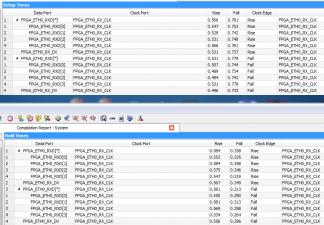
- Mark as New
- Bookmark
- Subscribe
- Mute
- Subscribe to RSS Feed
- Permalink
- Report Inappropriate Content
Thank you Alex310. Micrel PHY MDIO ports can be driven in order to adjust IO timing as you reminded and it may resolve the problem; Nevertheless it works in some situations without PAD skew adjustment. LogicLock option could be a solution, if you are sure everything is correct. I want to know how to verify timing on every synthesis run. This is my problem. I have studied TimeQuest manuals and AN477. As I mentioned the report_timing command does not tell me if timings are met.
- Mark as New
- Bookmark
- Subscribe
- Mute
- Subscribe to RSS Feed
- Permalink
- Report Inappropriate Content
--- Quote Start --- Hi msj. I use phy Marvell 88E1111-BAB-1000 (on my own board) and Micrel KSZ9021RL/RN (on Terasic Cyclone V kit). This chips has internal DLL for TX and RX path (to MAC). Micrel's DLL is cool and magic! You may set CLK to Data and Clk to CTL delay with 0.2 ns precision! Register 260 (104h) - RGMII Clock and Control Pad Skew 260.11:8 rxdv_pad_skew RGMII RX_CTL PAD Skew Control (0.2ns/step) 0111 260.7:4 txc_pad_skew RGMII TXC PAD Skew Control (0.2ns/step) RW 0111 260.3:0 txen_pad_skew RGMII TX_CTL PAD Skew Control (0.2ns/step) RW 0111 Register 261 (105h) - RGMII RX Data Pad Skew 261.15:12 rxd3_pad_skew RGMII RXD3 PAD Skew Control (0.2ns/step) RW 0111 261.11:8 rxd2_pad_skew RGMII RXD2 PAD Skew Control (0.2ns/step) RW 0111 261.7:4 rxd1_pad_skew RGMII RXD1 PAD Skew Control (0.2ns/step) RW 0111 261.3:0 rxdO_pad_skew RGMII RXD0 PAD Skew Control (0.2ns/step) RW 0111 You may see Altera an477 about constraining RGMII. Try use LogicLock option. See Timequest. My project report:http://www.alteraforum.com/forum/attachment.php?attachmentid=11840&stc=1 . Difference between lines must be <<1ns! (My project for Cyclone V and my own board) --- Quote End --- Hi Alex. Can you copy/paste your scd file to constraints the rgmii interface of the marvell chip? I have problems with cyclone5 and marvell PHY input constraints.
- Subscribe to RSS Feed
- Mark Topic as New
- Mark Topic as Read
- Float this Topic for Current User
- Bookmark
- Subscribe
- Printer Friendly Page