Hi,
I have some questions about the ARRIA10 SoC EMIF. The hardware board is designed by myself. The SoC is 10AS016E4F27E3SG, the DDR3 chip is MT41K256M16TW-107:P, and the DDR3 is connected to Bank 2K (the differential or single-ended external crystal clock source is not designed on this Bank). In the platform designer I made the following connection:Since I didn't connect the differential clock outside BANK 2K, I added the clock_bridge ip. I connected the out_clk of the clock bridge to the pll_ref_clk. There was no error in the platform designer. I assign the clock_in pin to the single-ended clock on the FPGA,When I compile the project,there are the following errors: Error(14566): The Fitter cannot place 1 periphery component(s) due to conflicts with existing constraints (1 REFCLK_GROUP(s)). Fix the errors described in the submessages, and then rerun the Fitter. The Intel FPGA Knowledge Database may also contain articles with information on how to resolve this periphery placement failure. Review the errors and then visit the Knowledge Database at https://www.altera.com/support/support-resources/knowledge-base/search.html and search for this specific error message number. Error(175020): The Fitter cannot place logic REFCLK_GROUP that is part of Generic Component ARRIA10_emif_a10_hps_0 in region (38, 5) to (38, 98), to which it is constrained, because there are no valid locations in the region for logic of this type. In this case, what suggestions can be set to generate pll_ref_clk clock, so as to achieve the DDR3 read and write control.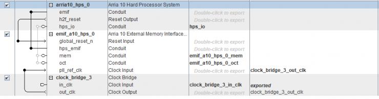
链接已复制
0 回复数