- Mark as New
- Bookmark
- Subscribe
- Mute
- Subscribe to RSS Feed
- Permalink
- Report Inappropriate Content
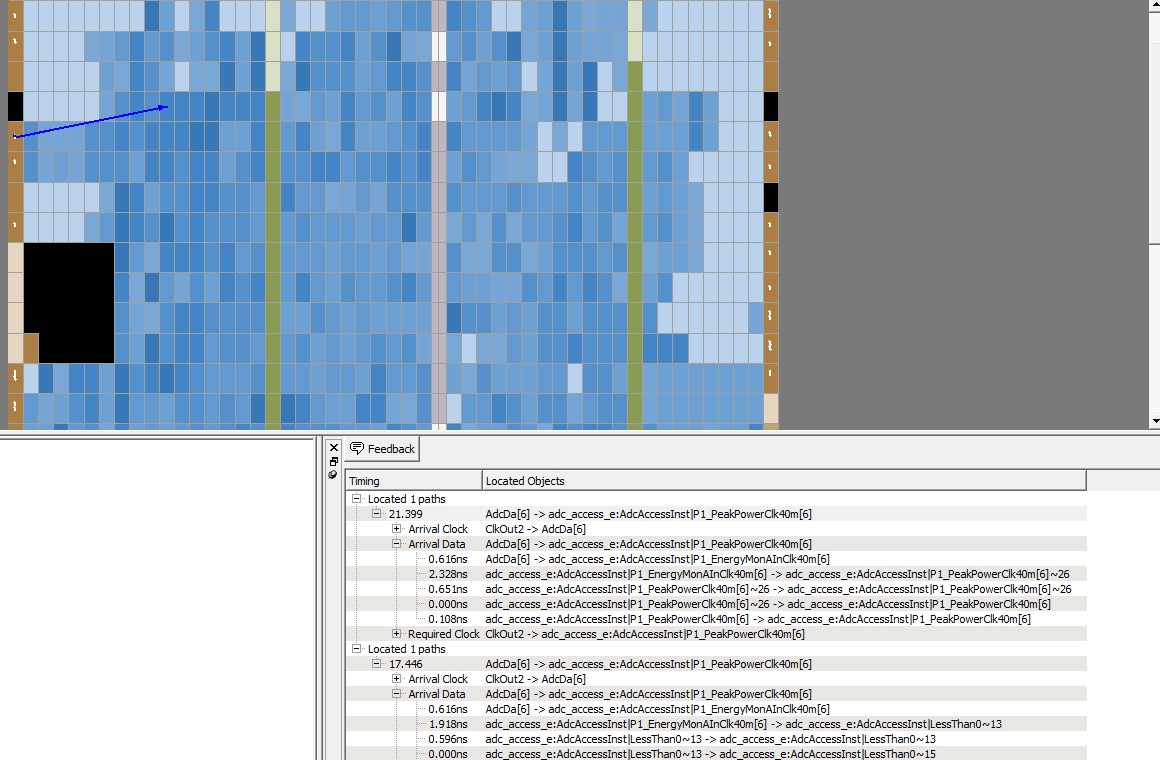
Hello, when I analyse the path from P1_EnergyMonAInClk40m[6] to P1_PeakPowerClk40m[6] for example in my design using Report Timing in TimeQuest 2 paths are reported with different timing delays. The attached timing report screenshots and chip planner show what is happening.
P1_EnergyMonAInClk40m[6] is clocked in from I/O pin AdcDa[6] on the rising edge of a 40MHz clock.
The device is a Cyclone 2 EP2C15AF256C8 and I use Quartus II 12 service pack 2 web edition.
Any ideas why the 2 paths are reported?
Thanks,
Clive
- Mark as New
- Bookmark
- Subscribe
- Mute
- Subscribe to RSS Feed
- Permalink
- Report Inappropriate Content
Link Copied
- Mark as New
- Bookmark
- Subscribe
- Mute
- Subscribe to RSS Feed
- Permalink
- Report Inappropriate Content
False alarm. There are 2 possible data paths in my design!
- Mark as New
- Bookmark
- Subscribe
- Mute
- Subscribe to RSS Feed
- Permalink
- Report Inappropriate Content
Let me know if there is any other concern regarding this.
- Mark as New
- Bookmark
- Subscribe
- Mute
- Subscribe to RSS Feed
- Permalink
- Report Inappropriate Content
I now transition this thread to community support. If you have a new question, Please login to https://supporttickets.intel.com/, view details of the desire request, and post a feed/response within the next 15 days to allow me to continue to support you. After 15 days, this thread will be transitioned to community support. The community users will be able to help you on your follow-up questions.
p/s: If any answer from community or Intel support are helpful, please feel free to mark as solution, give Kudos and rate 5/5 survey
- Subscribe to RSS Feed
- Mark Topic as New
- Mark Topic as Read
- Float this Topic for Current User
- Bookmark
- Subscribe
- Printer Friendly Page