- Mark as New
- Bookmark
- Subscribe
- Mute
- Subscribe to RSS Feed
- Permalink
- Report Inappropriate Content
Hello,
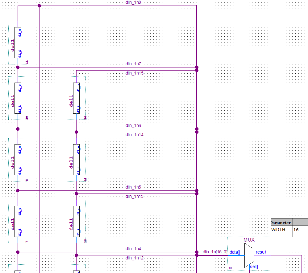
I have a FPGA design where LCELL primitives are used back to back to generate delay.

Each of the del1 block has a LCELL as below:

My question is: What is the amount of delay generated by LCELL? How can I implement the same functionality (generate same delay) without LCELL?
Link Copied
- Mark as New
- Bookmark
- Subscribe
- Mute
- Subscribe to RSS Feed
- Permalink
- Report Inappropriate Content
It's a lot easier to add delay like this using timing constraints. You can use set_min_delay and set_max_delay in your .sdc file to set delay on paths anywhere in your design.
To answer your question, you'd need to run a timing analysis to see what the delay is since it would be unique to the particular device and particular resource used to implement the delay.
- Mark as New
- Bookmark
- Subscribe
- Mute
- Subscribe to RSS Feed
- Permalink
- Report Inappropriate Content
To provide some extra info:
This schematic file is purely combinational with 16 back to back LCELLs and each LCELL's output is given to 16:1 Multiplexer. There are only 2 inputs to this file: a) the signal to which delay is generated and b) the 4 bit select input to the MUX.
As you mentioned the delay is unique to particular device, I would like to tell that this was initially implemented on old generation FPGAs in MAXPLUS. I am porting the design to latest Cyclone 10 family. So, I assume the delay generated on old FPGAs are different compared to Cyclone 10 device, hence the number of LCELLs used must be changed.
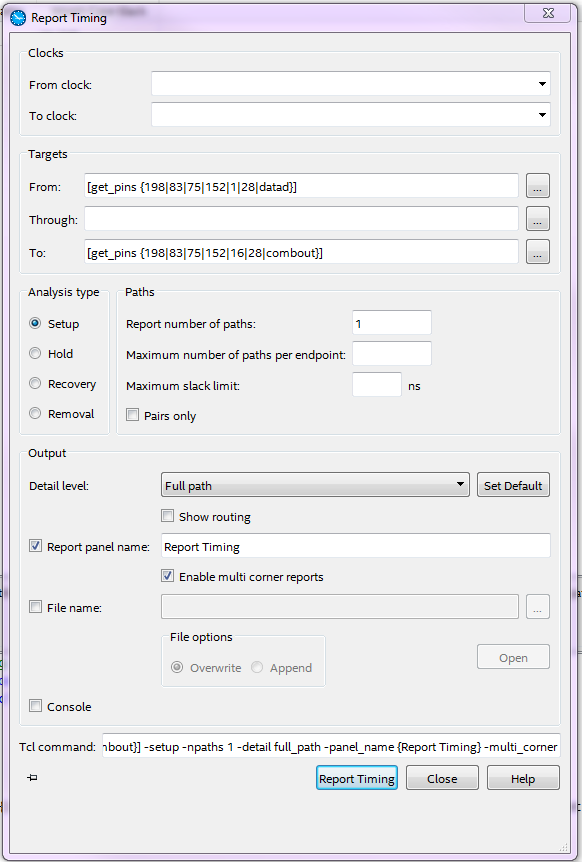
Could you please elaborate a little more on how to see the delay after timing analysis. In Timequest timing analyser, I used the "Report Timing" option in the Tasks window and I do not know what clock to provide in the dialog box that opens.

From: 198-83-75-152-1-28-datad :
28 is the block number of LCELL; 1 is the 1st instance of the LCELL; datad is the name of input pin to first LCELL.
TO: 198-83-75-152-16-28-combout:
28 is the block number of LCELL; 16 is the 16th instance of LCELL; combout is the name of output pin of 16th LCELL.
When I click Report timing without providing the clock, I get the reply from the tool as "Nothing to report".
- Mark as New
- Bookmark
- Subscribe
- Mute
- Subscribe to RSS Feed
- Permalink
- Report Inappropriate Content
To provide some extra info:
This schematic file is purely combinational with 16 back to back LCELLs and each LCELL's output is given to 16:1 Multiplexer. There are only 2 inputs to this file: a) the signal to which delay is generated and b) the 4 bit select input to the MUX.
As you mentioned the delay is unique to particular device, I would like to tell that this was initially implemented on old generation FPGAs in MAXPLUS. I am porting the design to latest Cyclone 10 family. So, I assume the delay generated on old FPGAs are different compared to Cyclone 10 device, hence the number of LCELLs used must be changed.
Could you please elaborate a little more on how to see the delay after timing analysis. In Timequest timing analyser, I used the "Report Timing" option in the Tasks window and I do not know what clock to provide in the dialog box that opens (see attachment).
From the picture:
From: 198-83-75-152-1-28-datad :
28 is the block number of LCELL; 1 is the 1st instance of the LCELL; datad is the name of input pin to first LCELL.
TO: 198-83-75-152-16-28-combout:
28 is the block number of LCELL; 16 is the 16th instance of LCELL; combout is the name of output pin of 16th LCELL.
- Mark as New
- Bookmark
- Subscribe
- Mute
- Subscribe to RSS Feed
- Permalink
- Report Inappropriate Content
You don't technically have to provide a clock to generate a timing report, but since timing analysis is based off a register to register model, that might not help you here. Do you have any registers around this logic or is the logic connected to I/O? You could generate a timing report from an input to an output of the device, going through the combinational logic in question.
Your best bet then is to use set_min_delay and set_max_delay as I mentioned which set absolute delays for any path in a design.
- Mark as New
- Bookmark
- Subscribe
- Mute
- Subscribe to RSS Feed
- Permalink
- Report Inappropriate Content
Hello,
I used the report Path command from the input to the schematic block to the output pin of FPGA and could get the timing information on every signal in the schematic. I have attached the report as excel file. But I see that the Multiplexer 54 is not appearing in the timing report. It is the only path for the signal to travel outside the attached schematic. Kindly refer the screenshots of .bdf file (aslo Zoomed ones for better viewing. This platform doesn't allow me to upload a BDF file) and also the remarks mentioned in the excel sheet.
I have also attached the screenshot of the RTL viewer. Does the RTL viewer show the exact implementation as in the BDF file? I do not see a serial connection of LCELLs. Please comment on this too.
I hope my explanation is clear.
- Mark as New
- Bookmark
- Subscribe
- Mute
- Subscribe to RSS Feed
- Permalink
- Report Inappropriate Content
Since this thread had been answered, we shall close this thread. If you still need further assistance, you are welcome to post a response within 15days or open a new thread, some one will be right with you. After 15 days, this thread will be transitioned to community support. The community users will be able to help you with your follow-up questions.
- Subscribe to RSS Feed
- Mark Topic as New
- Mark Topic as Read
- Float this Topic for Current User
- Bookmark
- Subscribe
- Printer Friendly Page