- Mark as New
- Bookmark
- Subscribe
- Mute
- Subscribe to RSS Feed
- Permalink
- Report Inappropriate Content
What is the initial state of the EPM1270F256I5 before the first programming? I'm trying to determine how to bias it.
Link Copied
- Mark as New
- Bookmark
- Subscribe
- Mute
- Subscribe to RSS Feed
- Permalink
- Report Inappropriate Content
Hi Noah,
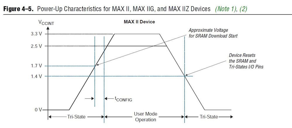
MAX II is having hot socketing feature in which you can drive the device during power up or power down. Meanwhile the IO is in tri-state state during device power on.
Regards,
YL
- Mark as New
- Bookmark
- Subscribe
- Mute
- Subscribe to RSS Feed
- Permalink
- Report Inappropriate Content
Hi YL,
To clarify, do the I/O pins STAY in tri-state after power-up (but pre-programming)?
Also, what state are the DEV_OE and DEV_CLRn pins in after power-up (but pre-programming)?
Thanks,
Noah
- Mark as New
- Bookmark
- Subscribe
- Mute
- Subscribe to RSS Feed
- Permalink
- Report Inappropriate Content
Hi Noah,
IO pins will not stay in tri-state after power-up. It will follows what you have programmed and set in Quartus.
DEV_CLRn are low by default after power-up. Meanwhile for DEV_OE, it has to be asserted so that the other IO pin will not remain in tri-state mode.
https://www.intel.com/content/dam/www/programmable/us/en/pdfs/literature/hb/max2/max2_mii5v1.pdf (Page 51)
Regards,
YL
- Mark as New
- Bookmark
- Subscribe
- Mute
- Subscribe to RSS Feed
- Permalink
- Report Inappropriate Content
Hi YL,
I'm asking because my intent is to perform environmental testing with simple biasing for my organization. Due to time/money constraint, I won't be programming the PLD before or during testing.
The reason I ask about the DEV_CLRn and DEV_OE pins is that they both have alternate modes as I/O pins. Without any programming, will pins M8 and M9 (for the FBGA-256 package) be in DEV_OE and DEV_CLRn modes respectively? Or will they be in the I/O mode?
Thanks,
Noah
- Mark as New
- Bookmark
- Subscribe
- Mute
- Subscribe to RSS Feed
- Permalink
- Report Inappropriate Content
To clarify, I'm wondering what the state of those two pins will be in in User-Mode Operation if during t_CONFIG, the CPLD isn't configured.
- Mark as New
- Bookmark
- Subscribe
- Mute
- Subscribe to RSS Feed
- Permalink
- Report Inappropriate Content
Hi Noah,
By default, both the pin are I/O pin. You will need to set them in Quartus if you want to have dev_clrn and dev_oe feature enabled.
So, I/O pin will be in tri-stated. For unused pin, which you do not configure anything on the pin, by default is in tri-state mode. However, it can be changed depending on your Quartus design. To check your unused pin state in user-mode, kindly go to:
Assignment -> Device -> Device Pin & Options -> Unused Pin
Regards,
YL
- Mark as New
- Bookmark
- Subscribe
- Mute
- Subscribe to RSS Feed
- Permalink
- Report Inappropriate Content
Hi YL,
Thanks, that's helpful. So to clarify, what you're saying is that:
- The IO/DEV_CLRn and IO/DEV_OE dual purpose pins by default will be in IO mode.
- All IO pins are always in tri-state mode during power-on.
- Unless I configure the IO pins differently, all will be in tri-state mode once the device has reached user mode.
Does that sound accurate? Also, would you say that the IO/GCLKx pins are also in IO mode by default?
Thanks,
Noah
- Mark as New
- Bookmark
- Subscribe
- Mute
- Subscribe to RSS Feed
- Permalink
- Report Inappropriate Content
Hi Noah,
For GCLK pin, you can assign input clock source to them and do some setting on Quartus.
https://www.intel.com/content/dam/www/programmable/us/en/pdfs/literature/an/an428.pdf (Page 13)
Else, it will be used as I/O pin.
Regards,
YL
- Mark as New
- Bookmark
- Subscribe
- Mute
- Subscribe to RSS Feed
- Permalink
- Report Inappropriate Content
So are they I/O pins or GCLK pins at default? Remember, I'm not programming my part.
- Mark as New
- Bookmark
- Subscribe
- Mute
- Subscribe to RSS Feed
- Permalink
- Report Inappropriate Content
Hi Noah,
They are IO by default.
Thank You.
- Subscribe to RSS Feed
- Mark Topic as New
- Mark Topic as Read
- Float this Topic for Current User
- Bookmark
- Subscribe
- Printer Friendly Page
